Semiconductor Device Using An Aluminum Interconnect To Form Through-Silicon Vias

Inactive Publication Date: 2011-02-17
IBM CORP
View PDF7 Cites 0 Cited by
  • Summary
  • Abstract
  • Description
  • Claims
  • Application Information

AI Technical Summary

Benefits of technology

[0010]In another aspect, an aluminum lateral interconnect in the BEOL uses an aluminum interconnect to determine the X and Y dimensions of a TSV, the TSV being a large feature when compared to the BEOL interconnects. The present invention provides a method and a structure that avoids problems associated with topography. The inventive aluminum feature limits the size, i.e., the X and Y dimensions of the TSV, and can be also be used as a BEOL conductor.
[0011]In still another aspect, the invention uses a layer of aluminum in the BEOL that controls the overlay and the critical dimensions. Since the TSV etch is devoid of chlorine in the plasma chemistry, etching will not affect the aluminum. By shaping the aluminum in an annular configuration, the entire annulus can be utilized to determine the placement (overlay) and the critical dimensions (CD). The width of the annulus can be made larger or smaller. If the width is made larger, it will facilitate the lithographic overlay, enabling a manufacturer to use less advanced equipment and consumables and making the process less expensive.
[0012]In yet another aspect of the invention, an aluminum/dielectric stack hard mask forms the TSV, leaving a portion of the hard mask for interconnecting the TSV to the BEOL. This hard mask allows to consume all

Problems solved by technology

Though much effort has been expended by practitioners working on making through-silicon vias (TSV) for various technology offerings, there are few that are presently in manufacturing.
A problem arises if a TSV is required to connect the chip interconnects within the die or chip.
This can be achieved with multiple steps, however with the addition of these steps there is associated yield loss and expense.
Furthermore, if there is the requirement of a passive element that needs to be fabricated after the TSV, it can become problematic because of t

Method used


Image

  • Semiconductor Device Using An Aluminum Interconnect To Form Through-Silicon Vias
  • Semiconductor Device Using An Aluminum Interconnect To Form Through-Silicon Vias
  • Semiconductor Device Using An Aluminum Interconnect To Form Through-Silicon Vias

Examples


Example

[0029]For simplicity and clarity, elements shown in the drawings have not necessarily been drawn to scale. For example, the dimensions of some of the elements of particular interest may be exaggerated relative to other elements.

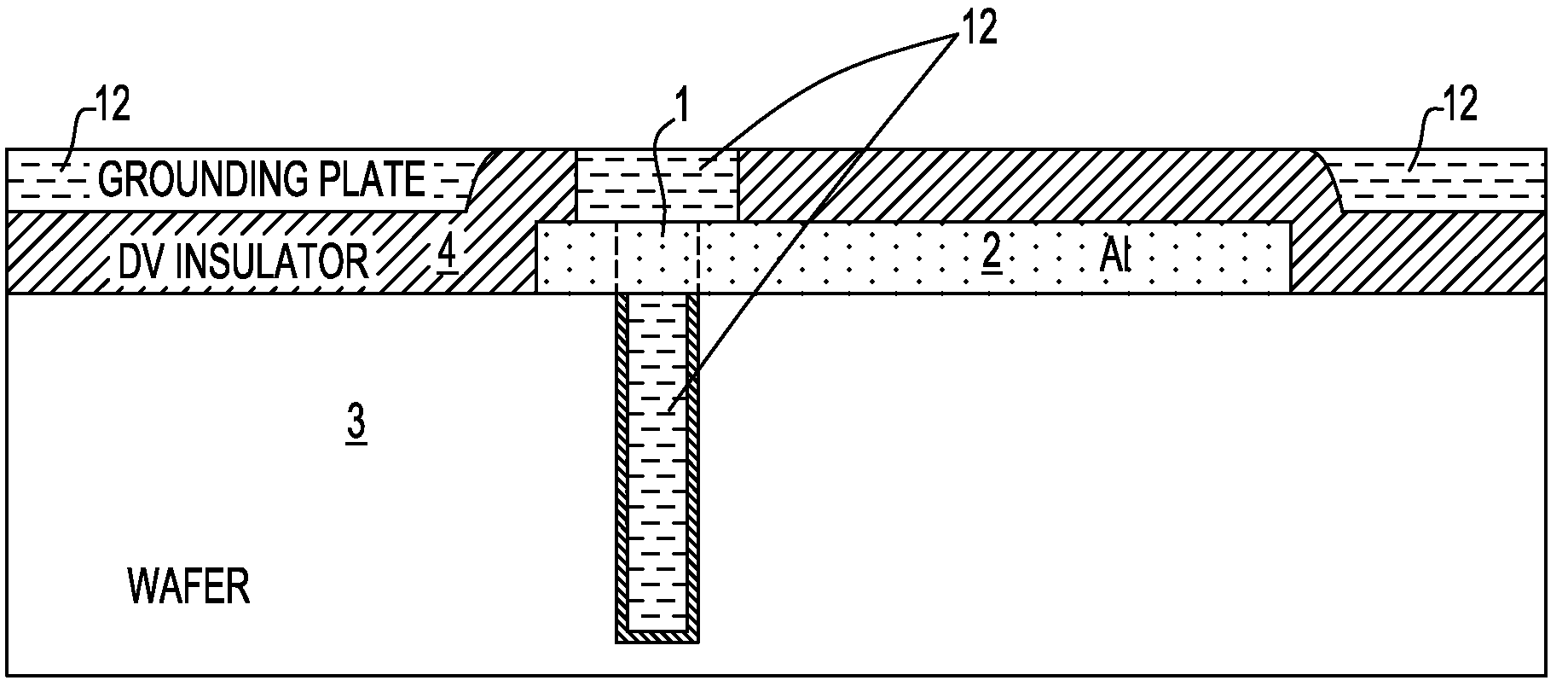
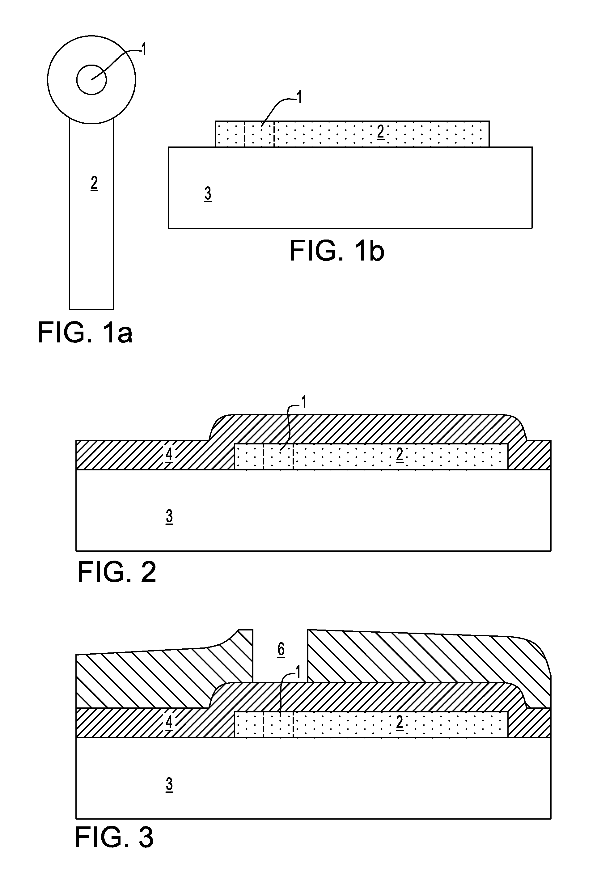
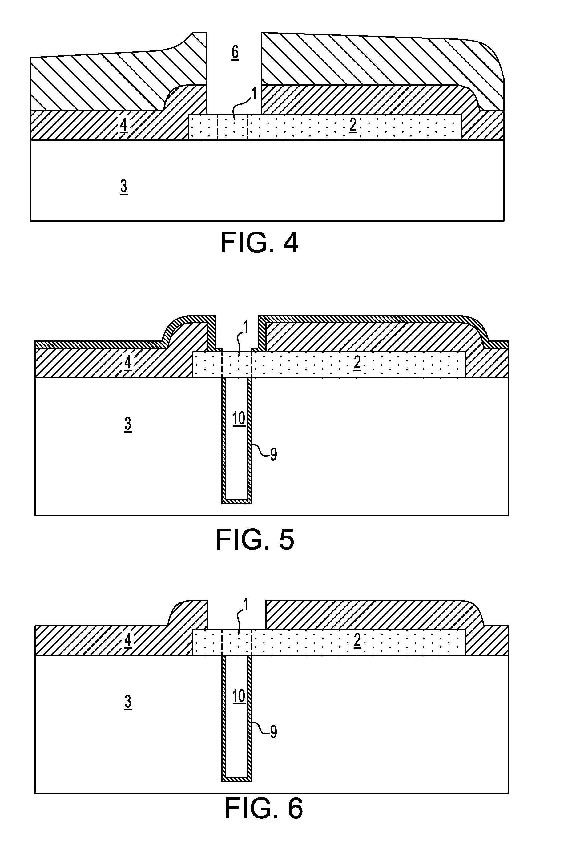
[0030]Referring to FIG. 1(a), a top-down illustration of an aluminum annulus 1 connected to an aluminum strap 2 is shown. In the etch process for the through-silicon via, the chemistry used has little or no effect on the aluminum since aluminum etching requires a chlorine based chemistry not present in a TSV etch. Preferably, the annulus 1 has a 20 μm opening in the center, and an aluminum width of 4 μm. The aforementioned dimensions can be achieved by utilizing a lithography tool having an overlay specification greater or equal to 4 μm, permitting to use less advanced photoresist, since the sidewall of the resist becomes irrelevant in view of the RIE being shaped by the aluminum annulus. Additionally, once the TSV is completed and filled with conductor mater...


PUM


Abstract

An aluminum lateral interconnect of a Back End of the Line (BEOL) is used to define the x and y dimensions of a through-silicon via in a semiconductor chip formed in a silicon substrate. The TSV includes one or more aluminum annulus formed on a surface of the substrate, and a deep trench in the substrate having a diameter that is determined by the diameter of the aluminum annulus. The annulus can also be provided with a conductive strap upon which a capacitor can be formed. The strap can also be used to provide a connection of the TV to other BEOL interconnects.

Description

FIELD OF THE INVENTION[0001]The present invention relates to a method and a structure for electrically interconnecting integrated circuit semiconductor devices, and more particularly, to the formation of interconnects having through-silicon vias formed by way of an aluminum deposition, facilitating the formation of passive devices in a Back End of Line of a semiconductor chip.BACKGROUND OF THE INVENTION[0002]Packaging technologies for a semiconductor integrated device have been continuously developed to satisfy the demands for mounting efficiency and miniaturization. Various semiconductor interconnect technologies have been developed as the miniaturization and high performance resulting from recent development trends in the semiconductor chip devices technology.[0003]Interconnects and packaging-related issues are among factors that determine not only the number of circuits that can be integrated in a semiconductor die or “chip,” but also the chip performance. These issues have gaine...

Claims


Application Information

Patent Timeline
IPC IPC(8): H01L29/92H01L23/48H01L21/02H01L21/768
CPCH01L21/76895H01L21/76898H01L23/481H01L23/5222H01L28/60H01L2924/0002H01L2924/00012H01L2924/00
Inventor PETRARCA, KEVIN S.ANGYAL, MATTHEWCLEVENGER, LAWRENCE A.RADENS, CARLSAPP, BRIAN C.
Owner IBM CORP
Why Eureka
Try Eureka