Display device and method of fabricating the same

a technology of display device and manufacturing method, which is applied in the manufacture of electrode systems, electric discharge tubes/lamps, instruments, etc., can solve the problems of polymer layer, adversely affecting subsequent process, unfavorable strain resistance, etc., and achieve the effect of simplifying the packaging process

Active Publication Date: 2012-05-17
AU OPTRONICS CORP
View PDF6 Cites 40 Cited by
  • Summary
  • Abstract
  • Description
  • Claims
  • Application Information

AI Technical Summary

Benefits of technology

[0005]It is therefore one of the objectives of the present invention to provide a display device and a method of fabricating the same display device to solve the existing problems and simplify the package process.
[0008]By virtue of the design of the display device according to the exemplary embodiment of the present invention, no warpage would occur in the high temperature process. In addition, the sealant is able to protect the periphery of the first side surface of the substrate, the periphery of the second side surface of the display medium layer, the driving component and the flexible printed circuit, and thus the package process is simplified.

Problems solved by technology

The small Young's modulus and the film thickness of the polymeric layers make the polymeric layers flexible, though; it is unfavorable to the strain resistance.
In the high temperature process, the difference of coefficient of thermal expansion (CTE) between the substrate and the polymeric layers causes warpage of the polymeric layers which adversely impacts subsequent process.
Specifically, the difference of CTE would induce serious stress residual, lead to the breaking of glass substrate, and lower the reliability, the yield and the productivity.
This additional package step complicates the package process of the conventional display device.

Method used


Image

  • Display device and method of fabricating the same
  • Display device and method of fabricating the same
  • Display device and method of fabricating the same

Examples


Embodiment Construction

[0017]To provide a better understanding of the present invention, preferred embodiments will be made in detail. The preferred embodiments of the present invention are illustrated in the accompanying drawings with numbered elements.

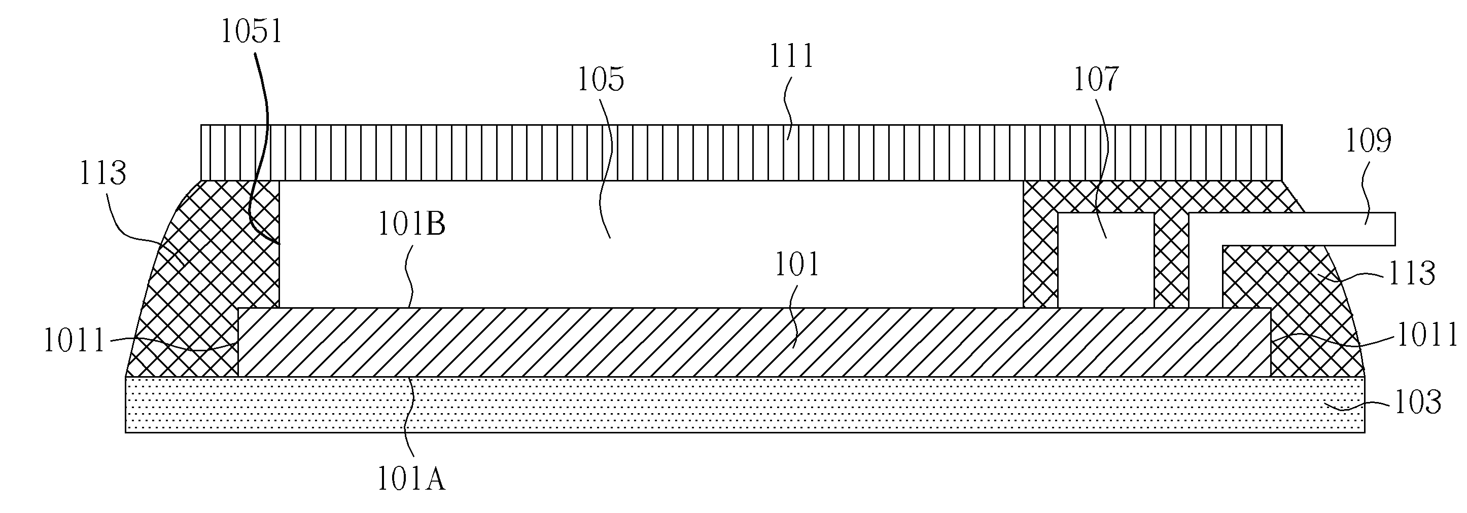
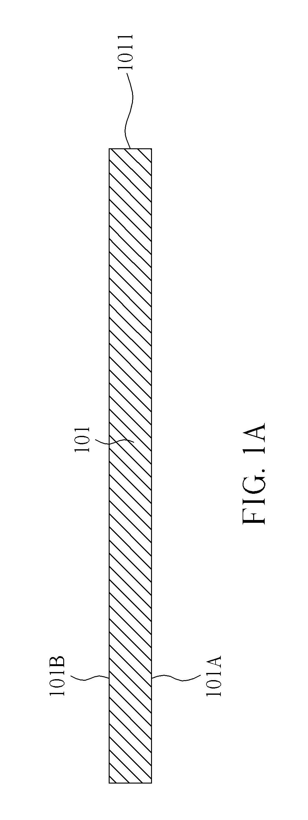
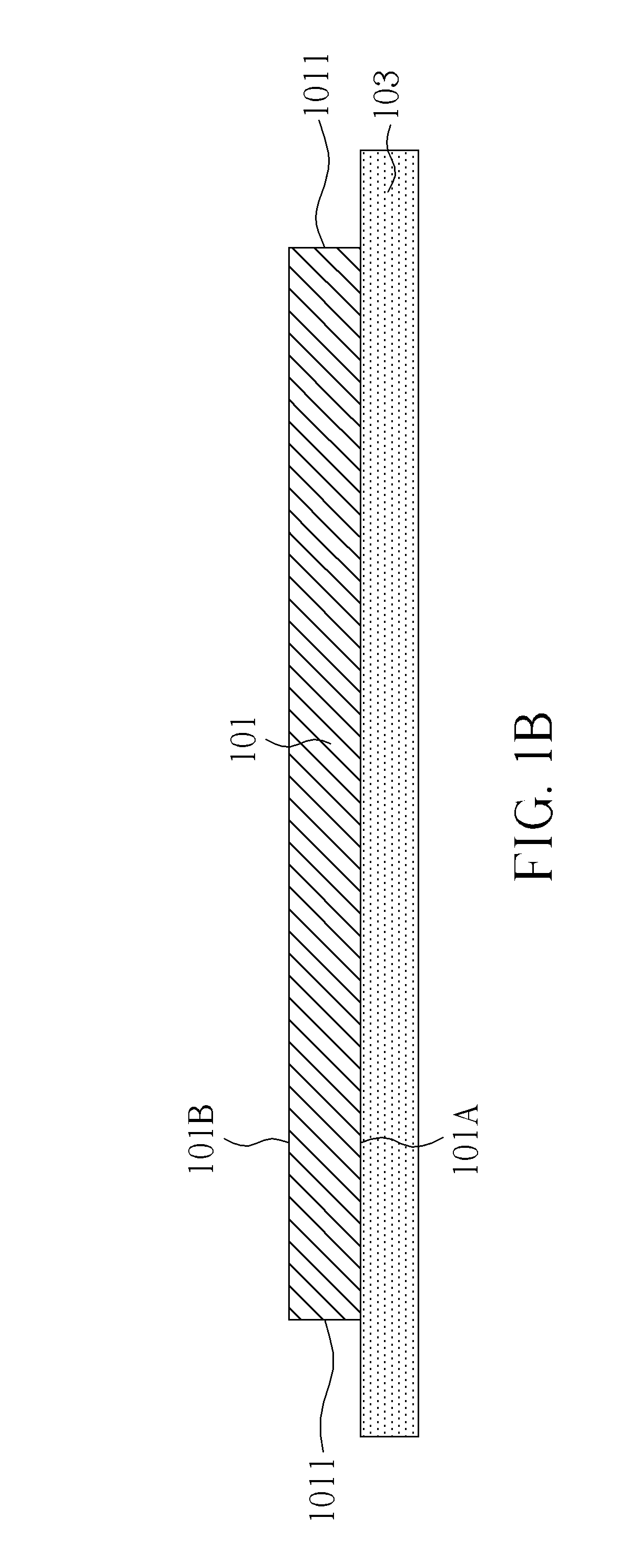
[0018]Please refer to FIG. 1A-FIG. 1F. FIG. 1A-FIG. 1F are cross-sectional views illustrating a display device according to a first exemplary embodiment of the present invention. As shown in FIG. 1A, a substrate 101 is provided. The substrate 101 may be a flexible substrate such as a plastic substrate, or a hard substrate such as a glass substrate or a quartz substrate. Additionally, the substrate 101 has a first surface (rear surface) 101A, a second surface (front surface) 101B and a first side surface 1011, wherein the first side surface 1011 is individually connected to the first surface 101A and the second surface 101B, and the first side surface 1011 is between the first surface 101A and the second surface 101B. The first side surface 1011 may be one ...


PUM

PropertyMeasurementUnit
flexibleaaaaaaaaaa
coefficient of thermal expansionaaaaaaaaaa
CTEaaaaaaaaaa

Abstract

A display device includes a substrate, a backplane, a display medium layer, a protective layer, a driving component, a flexible printed circuit (FPC) and a sealant. The backplane and the display medium layer are disposed on the lower side and the upper side of the substrate, respectively. The protective layer covers the display medium layer and prevents moisture and oxygen from permeating into the display medium layer to deteriorate its performance. The sealant surrounds the first side surface of the substrate and the second side surface of the display medium layer, and wraps at least a portion of the driving component and a portion of the FPC. Additionally, a manufacturing method of a display device is also provided.

Description

BACKGROUND OF THE INVENTION[0001]1. Field of the Invention[0002]The present invention is related to a display device and a method of fabricating the same display device, and more particularly, to a package structure of a flexible display device and the method of fabricating the same.[0003]2. Description of the Prior Art[0004]The conventional electrophoretic display device includes a substrate; a display medium layer used as a medium for image display; a protective layer used to insulate moisture and oxygen from the display medium layer; a sealant for packaging the periphery of the electrophoretic display device; and a driving component and a flexible printed circuit (FPC) used to drive the electrophoretic display device. After the driving component and the flexible printed circuit are individually connected to the substrate, mostly, a film of protection glue such as Tuffy glue would be coated on the driving component and a portion of flexible printed circuit for protection. Generall...

Claims


Application Information

Patent Timeline
Patent Type & Authority Applications(United States)
IPC IPC(8): G02F1/1339H01J9/26G02F1/167G02F1/1679
CPCG02F1/1339G02F1/167G02F1/13454G02F1/1679
Inventor WU, HO-CHIENPENG, CHIA-TIENHU, CHIH-JEN
Owner AU OPTRONICS CORP
Why Eureka
Try Eureka