Two terminal multi-layer thin film resistance switching device with a diffusion barrier and methods thereof

a technology of diffusion barrier and resistance switching device, which is applied in the direction of semiconductor devices, digital storage, instruments, etc., can solve the problems of resistance change, poor retention, and change the resistance state of the device, so as to prevent back motion and mitigate the challenge of resistance change devi

Active Publication Date: 2012-05-24
UNIV HOUSTON SYST
View PDF4 Cites 29 Cited by
  • Summary
  • Abstract
  • Description
  • Claims
  • Application Information

AI Technical Summary

Benefits of technology

[0009]The retention challenge in resistance change devices can be mitigated by preventing the back motion of ions / vacancies after they have been moved by the application of an electric field. An electric-pulse-induced-resistance change device (EPIR device) is provided which is a resistance switching device. It has a buffer layer inserted between a first active resistance switching layer and a second active resistance switching layer, with both active switching layers connected to electrode layers directly or through additional buffer layers between the active resistance switching layers and the electrodes. This device in its simplest form has the structure: electrode-active layer-buffer layer-active layer-electrode.

Problems solved by technology

The changing concentration of vacancies within this interface region affects the conductivity of the perovskite oxide and results in resistance change.
This change in concentration, however, results in a chemical potential gradient which under certain conditions can become a driver in changing the concentration of oxygen ions or vacancies between the interface region and the bulk, thus changing the resistance state of the device and yielding poor retention.

Method used


Image

  • Two terminal multi-layer thin film resistance switching device with a diffusion barrier and methods thereof
  • Two terminal multi-layer thin film resistance switching device with a diffusion barrier and methods thereof
  • Two terminal multi-layer thin film resistance switching device with a diffusion barrier and methods thereof

Examples


Embodiment Construction

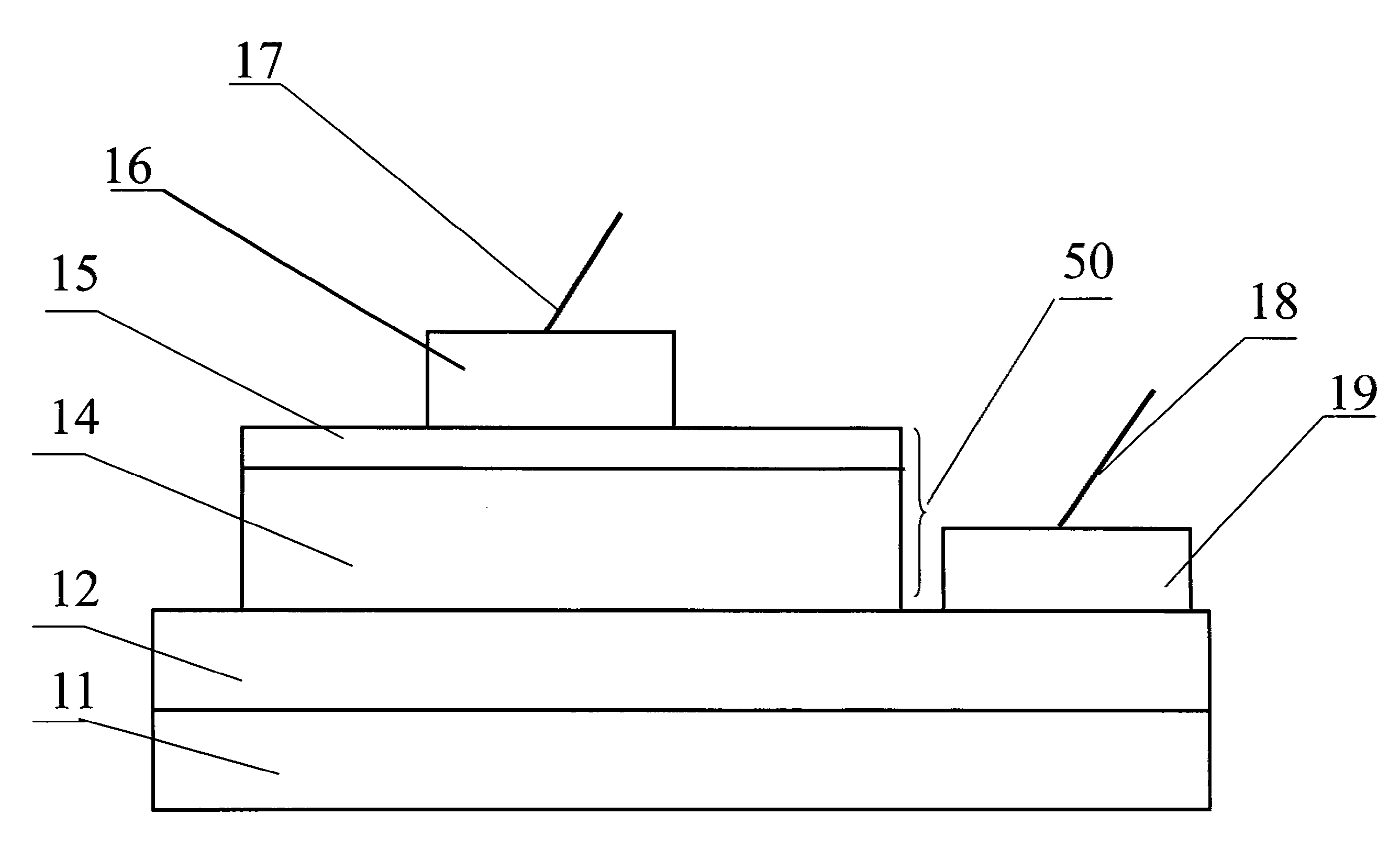
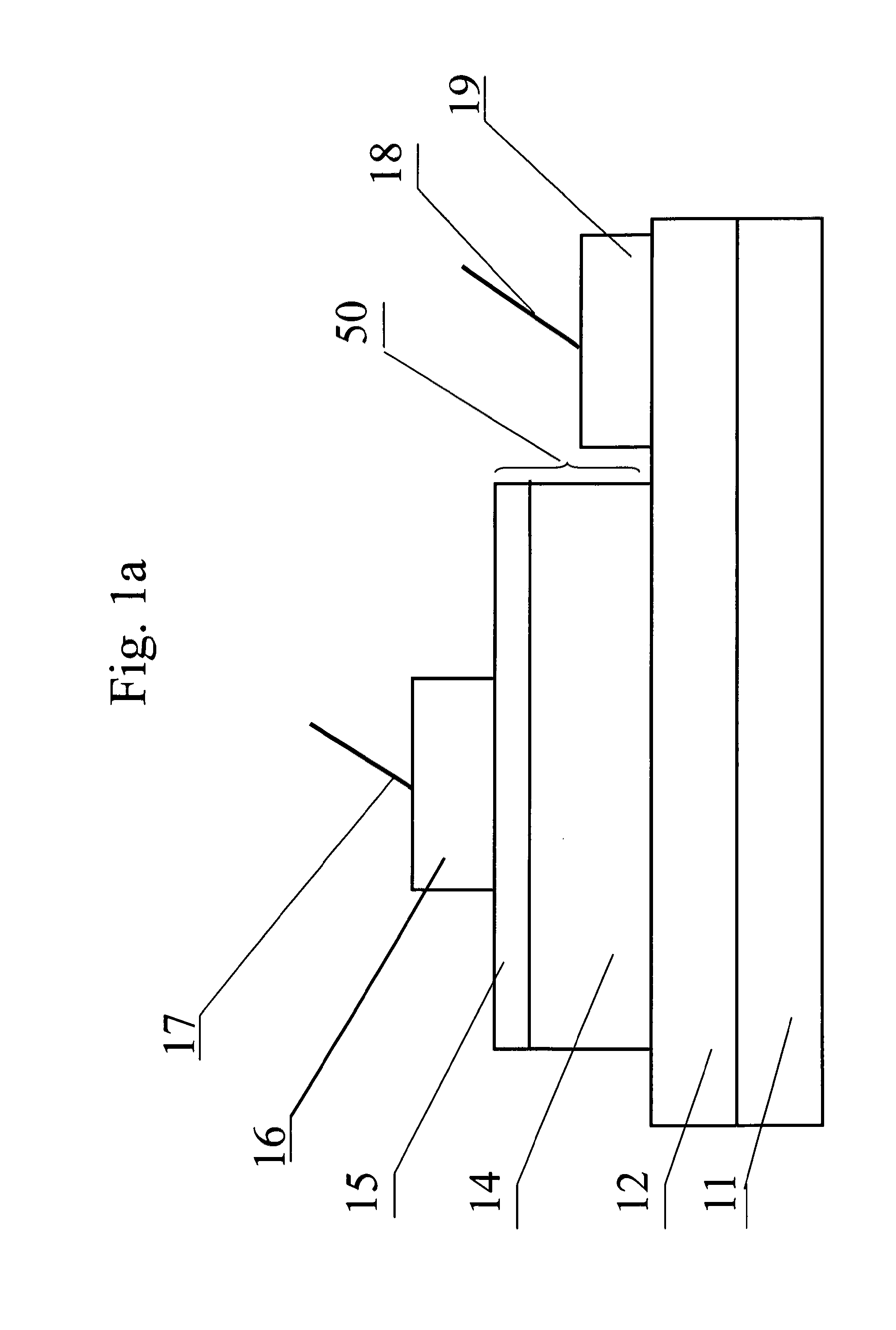
[0027]In summary, buffer layers are added to a resistance switching device to create a buffered resistance switching device. Referring to FIG. 1a, a bottom conductive electrode layer 12 is used as the bottom electrode layer on substrate 11. A thin top switchable function film, or layer, 14 partially covers the bottom conductive electrode layer 12. A bottom electrode contact pad 19 is connected to the bottom conductive electrode layer 12. The top switchable function layer 14 is covered with a top buffer layer 15. The top switchable function layer 14 and top buffer layer 15 form a multi-layer structure 50. A top electrode contact pad 16 is fabricated on top of the top buffer layer 15. Electrode contact pads 16 and 19 are connected to wires 17 and 18, respectively. The conductive electrode layer 12 and the top electrode contact pad 16 may be crystalline or polycrystalline conducting oxide or metallic layers.

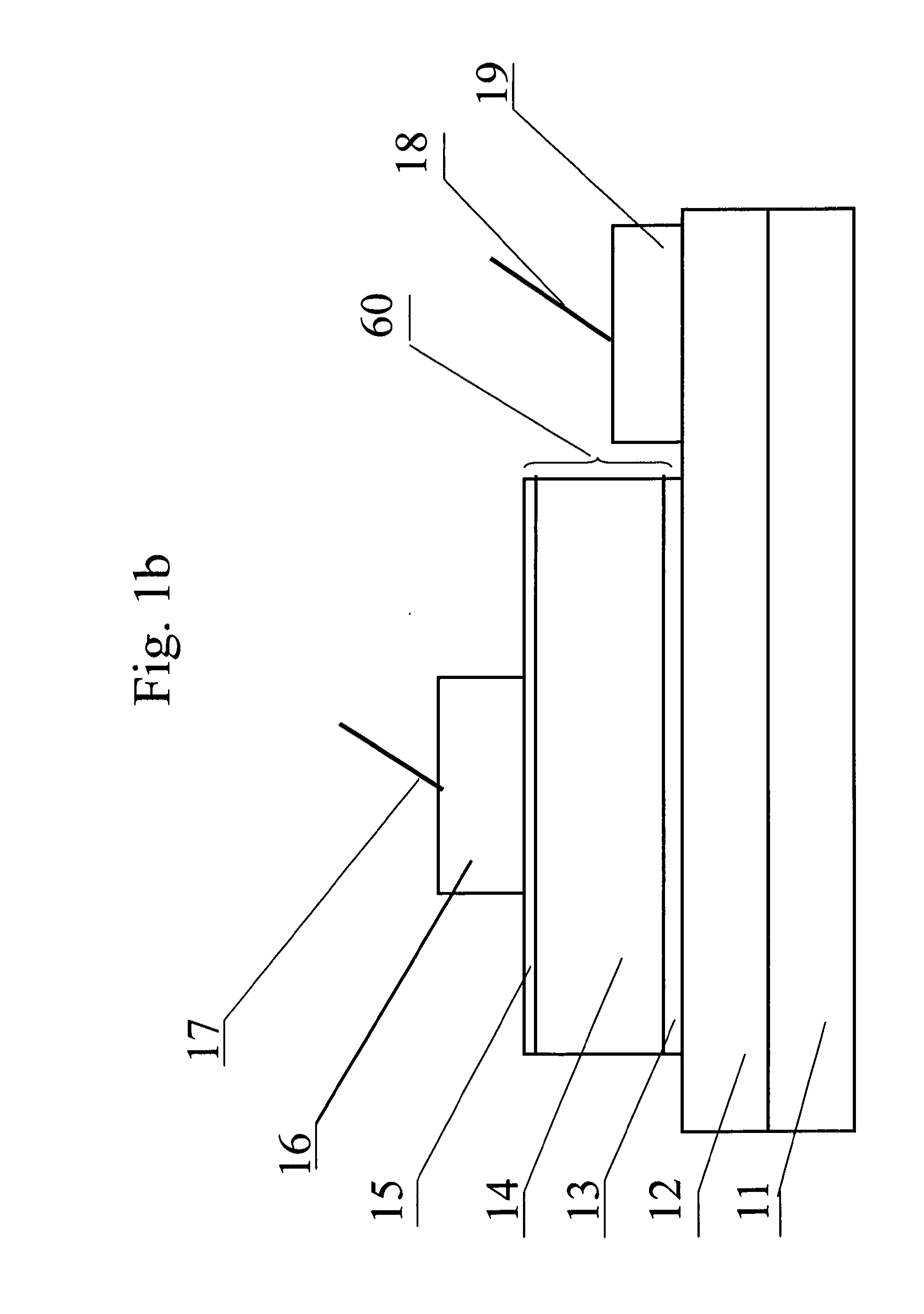
[0028]Referring to FIG. 1b, the individual components and their arrangements in...


PUM


Abstract

An electric-pulse-induced-resistance change device (EPIR device) is provided which is a resistance switching device. It has a buffer layer inserted between a first active resistance switching layer and a second active resistance switching layer, with both active switching layers connected to electrode layers directly or through additional buffer layers between the active resistance switching layers and the electrodes. This device in its simplest form has the structure: electrode-active layer-buffer layer-active layer-electrode. The second active resistance switching layer may, in the alternative, be an ion donating layer, such that the structure becomes: electrode-active layer-buffer layer-ion donating layer-electrode. The EPIR device is constructed to mitigate the retention challenge.

Description

CROSS-REFERENCE TO RELATED APPLICATIONS[0001]This application is a continuation in part of U.S. patent application Ser. No. 12 / 586,147, which is a divisional of U.S. application Ser. No. 11 / 034,695, filed on Jan. 13, 2005, which claims the benefit of U.S. Provisional Application No. 60 / 536,155, filed on Jan. 13, 2004.STATEMENT REGARDING FEDERALLY SPONSORED RESEARCH OR DEVELOPMENT[0002]Not Applicable.REFERENCE TO A “SEQUENTIAL LISTING,” A TABLE, OR A COMPUTER PROGRAM LISTING APPENDIX SUBMITTED ON A COMPACT DISC[0003]Not Applicable.BACKGROUND OF THE INVENTION[0004]1. Field of the Invention[0005]The present invention relates to a two-terminal microelectronic device, and, in particular, to a two-terminal non-volatile resistor device, having a structure of electrode / active-resistance change material-layer / electrode, which is an Electric-Pulse-Induced-Resistance change device, commonly referred to by the acronym EPIR.[0006]2. Description of the Related Art[0007]The electric resistance of ...

Claims


Application Information

Patent Timeline
Patent Type & Authority Applications(United States)
IPC IPC(8): H01L45/00H01L21/02
CPCG11C13/0007G11C13/0069G11C2013/0073G11C2213/31G11C2213/51G11C2213/56H01L45/147H01L45/08H01L45/085H01L45/12H01L45/1233H01L45/143H01C7/006H10N70/801H10N70/245H10N70/24H10N70/8825H10N70/8836H10N70/826G11C13/0021
Inventor IGNATIEV, ALEXWU, NAIJUANYOUNG-FISHER, KRISTINAEBRAHIM, RABI
Owner UNIV HOUSTON SYST
Why Eureka
Try Eureka