
Conductive films

a technology of conductive films and conductive strips, applied in the field of transparent conductive strips, can solve the problems of difficult implementation of other materials, high cost, and inability to withstand the effects of heat, and achieve the effects of improving the performance of the conductive strips, and improving the conductive performan

Inactive Publication Date: 2012-05-24
THE BOARD OF TRUSTEES OF THE LELAND STANFORD JUNIOR UNIV
View PDF25 Cites 87 Cited by
  • Summary
  • Abstract
  • Description
  • Claims
  • Application Information

AI Technical Summary

Benefits of technology

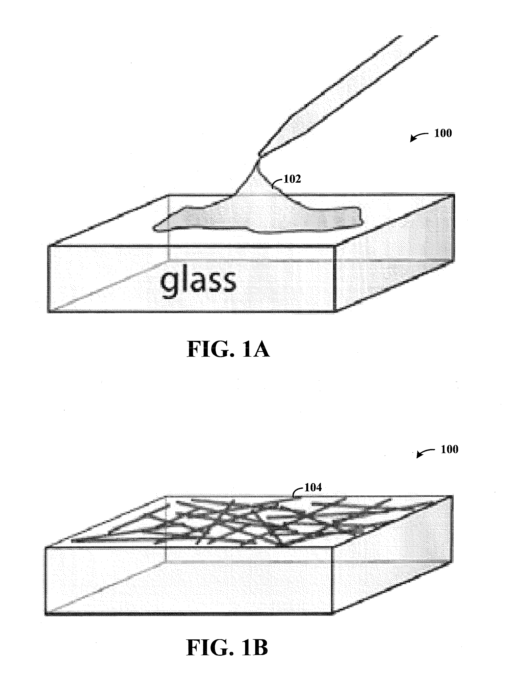
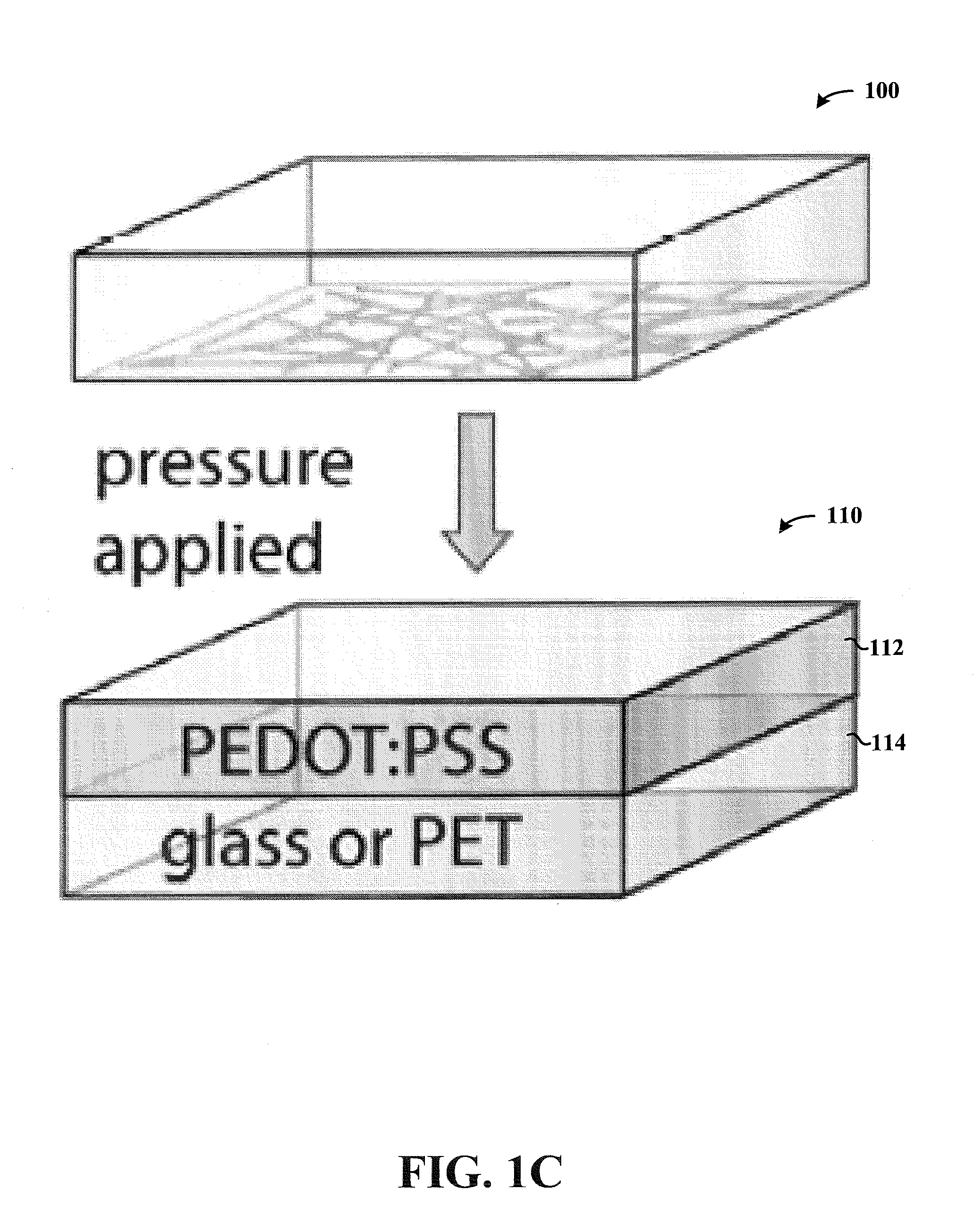
"The present invention is about devices, methods, and systems involving transparent conductive films that address challenges in the field of conductive materials in transparent films. The invention includes an organic substrate layer and an inorganic nanowire mesh embedded in the organic substrate layer. The embedded mesh can be used in various electronic devices that require conductive material in a transparent film. The invention also includes a method for forming a transparent conductive film by introducing a nanowire mesh to a polymer and embedding the mesh in the polymer. The invention further includes devices incorporating the nanowire mesh / polymer film, such as optoelectronic devices, photovoltaic devices, touch screens, solar cells, and organic-based light-emitting displays. The invention also includes methods for manufacturing devices incorporating the nanowire mesh / polymer film."

Problems solved by technology

However, ITO is relatively expensive, can be expensive to form, and can further be brittle.
Other materials have been difficult to implement, due to a variety of characteristics such as cost and difficulty in their implementation, or insufficient performance (e.g., insufficient transparency, insufficient conductivity, and related tradeoffs).
These and other issues remain as a challenge to a variety of methods, devices and systems that use or benefit from transparent conductive films.

Method used


Image

  • Conductive films
  • Conductive films
  • Conductive films

Examples


Embodiment Construction

[0023]The present invention relates to transparent and semi-transparent conductors as described herein. While the present invention is not necessarily limited, various aspects of the invention may be appreciated through a discussion of examples using these and other contexts. The following discussion, as well as that in the Appendices that form part of this patent document, describe various exemplary embodiments without limitation to other related embodiments and / or subject matter herein.

[0024]Various example embodiments are directed to solution-processed transparent conductors, which can be implemented on flexible substrates. Some embodiments are directed to a composite solution-processed material for forming transparent conductors used in optoelectronic devices. For some applications, the composite solution-processed material can be used in devices that have employed indium-tin-oxide material as a conductor.

[0025]As applicable with various embodiments, it has been discovered herew...


PUM

PropertyMeasurementUnit
diametersaaaaaaaaaa
RMS surface roughnessaaaaaaaaaa
diameteraaaaaaaaaa

Abstract

Conductive films with transparency characteristics are provided. In accordance with various example embodiments, a transparent conductive film includes an inorganic nanowire mesh embedded in an organic substrate layer. The embedding may involve, for example, embedding a majority of, or substantially all of the nanowire mesh in the organic substrate layer to facilitate a resulting surface roughness of the combined nanowire mesh-polymer that is less than a surface roughness of the mesh alone (e.g., or otherwise embedded), and in turn facilitates desirable conductivity characteristics.

Description

RELATED PATENT DOCUMENT[0001]This patent document claims benefit under 35 U.S.C. §119 to U.S. Provisional Patent Application Ser. No. 61 / 369,493, entitled “Transparent Conductive Films” and filed on Jul. 30, 2010; this patent document and the Appendices filed in the underlying provisional application, including the references cited therein, are fully incorporated herein by reference.FIELD[0002]The present invention relates generally to conductors, and more specifically to transparent conductive films and methods therefore.BACKGROUND[0003]A variety of materials have been used for transparent conductors (conductors passing at least some, if not a majority, of light incident thereupon). Such conductors are used, for example, with optoelectronic devices, displays and touch screens. One type of material that has been used with these devices is tin-doped indium oxide (ITO). However, ITO is relatively expensive, can be expensive to form, and can further be brittle. Other materials have bee...

Claims


Application Information

Patent Timeline
Patent Type & Authority Applications(United States)
IPC IPC(8): G06F3/041G09G5/00B32B5/12B32B3/00B32B7/02G06F3/038B32B5/16H10K99/00
CPCB82Y20/00B82Y30/00H01L51/444H01L51/445H01L51/0037Y10T428/2495G06F3/041H01L51/442G06F3/0412Y10T428/24355Y02E10/549Y10T442/10H10K85/1135H10K30/821H10K30/83H10K30/82
Inventor GAYNOR, WHITNEYPEUMANS, PETER
Owner THE BOARD OF TRUSTEES OF THE LELAND STANFORD JUNIOR UNIV
Learn More