Group-iii nitride semiconductor laser device, and method of fabricating group-iii nitride semiconductor laser device

a laser device and nitride technology, applied in the direction of semiconductor lasers, laser optical resonator construction, laser details, etc., can solve the problems of unable to produce cavity mirrors by using conventional cleaved facets, unable to achieve laser waveguide orientation, and heavy process conditions

Inactive Publication Date: 2012-05-31
SUMITOMO ELECTRIC IND LTD
View PDF24 Cites 5 Cited by
  • Summary
  • Abstract
  • Description
  • Claims
  • Application Information

AI Technical Summary

Benefits of technology

[0023]In the semiconductor laser using end faces different form cleavage facets for an optical cavity, light returning to the semiconductor laser has a great influence on lasing characteristics of the semiconductor laser, and makes the operation of the semiconductor laser instable. This requires a module implementing a nitride semiconductor laser to have an optical isolator therein. The addition of the optical isolator increases the cost of the module. Returning components are created by optical parts (such as lens, filter, and mirror) when a laser beam from the nitride semiconductor laser passes therethrough. These return components return to the waveguide of the nitride semiconductor laser and make the nitride semiconductor laser instable.
[0067]When the primary surface has the slight slant from these typical semipolar planes, it is also feasible to provide the first and second end faces with flatness and perpendicularity enough to construct the laser cavity of the III-nitride semiconductor laser device, or without ion damage.

Problems solved by technology

However, this orientation of the laser waveguide does not allow use of the conventional cleaved facets such as c-planes, a-planes, or m-planes for the cavity mirrors.
It becomes a heavy burden to derive process conditions for obtaining good dry-etched facets in the current technical level.
However, as described above, where the laser waveguide is directed so as to extend in the inclination direction (off-axis direction) of the c-axis, the cavity mirrors cannot be produced by making use of the conventional cleaved facets.

Method used


Image

  • Group-iii nitride semiconductor laser device, and method of fabricating group-iii nitride semiconductor laser device
  • Group-iii nitride semiconductor laser device, and method of fabricating group-iii nitride semiconductor laser device
  • Group-iii nitride semiconductor laser device, and method of fabricating group-iii nitride semiconductor laser device

Examples


example 1

[0144]A semipolar-plane GaN substrate is prepared and perpendicularity of a fractured face is observed as described below. A {20-21}-plane GaN substrate is used as the substrate, which is cut at the angle of 75 degrees toward the m-axis out of a (0001) GaN ingot thickly grown by HVPE. The primary surface of the GaN substrate is mirror-finished, and the back surface is in a ground pear-skin state. The thickness of the substrate is 370 μm.

[0145]On the back side in the pear-skin state, a marking line is drawn perpendicularly to the direction of the projected c-axis onto the primary surface of the substrate with a diamond pen, and thereafter the substrate is fractured by press. For observing the perpendicularity of the resultant fractured face, the substrate is observed from the a-plane direction with a scanning electron microscope.

[0146]Part (a) of FIG. 8 shows a scanning electron microscope image of the fractured face observed from the a-plane direction, and the right end face is the ...

example 2

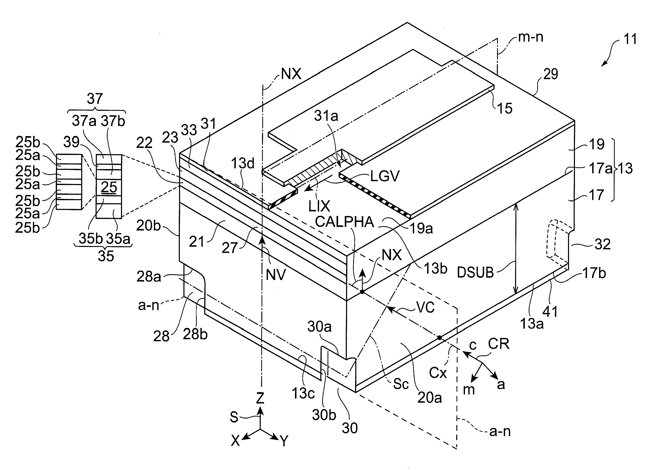
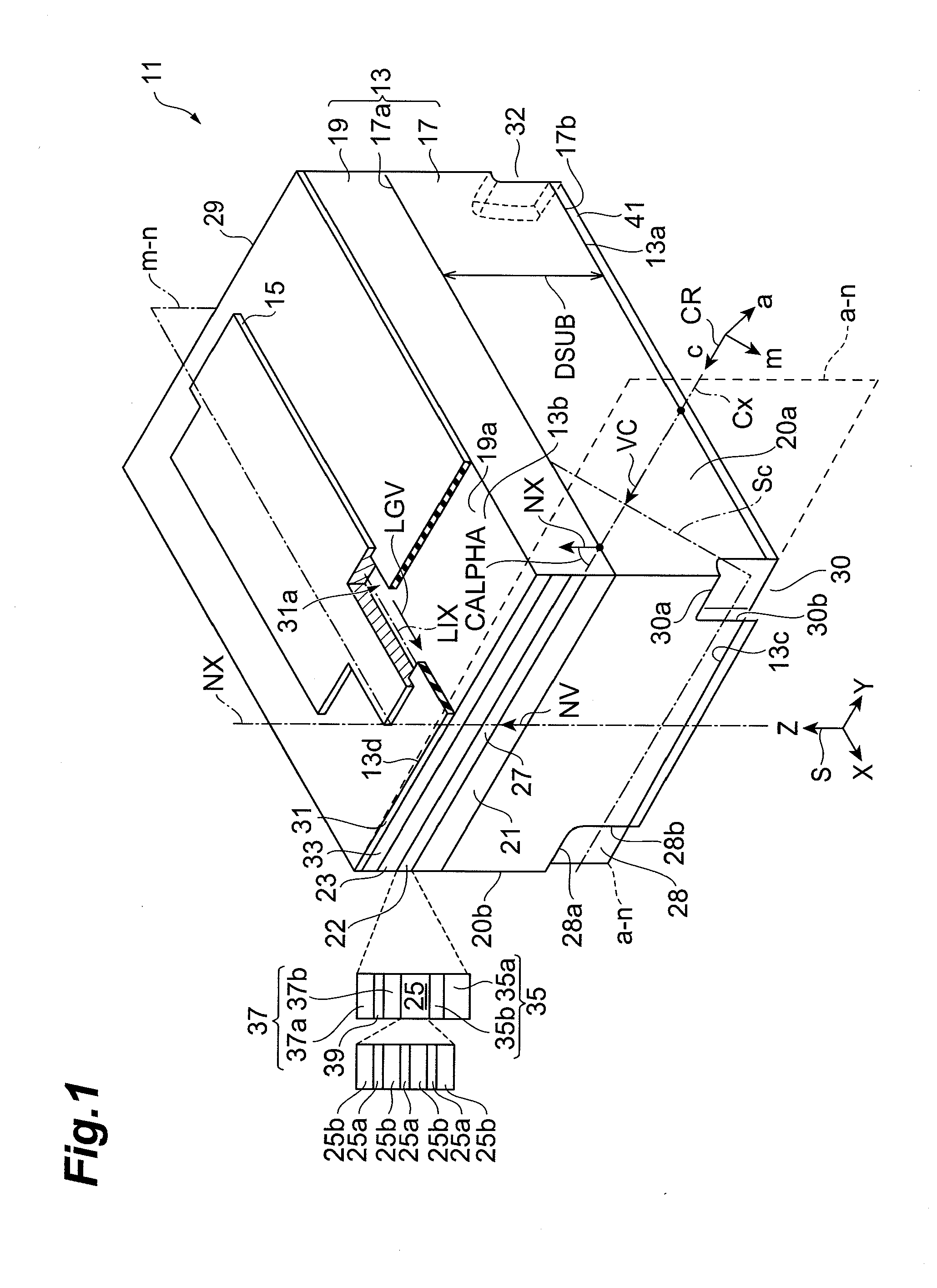
[0147]Example 1 shows that, in the GaN substrate having the semipolar {20-21} plane, the fractured face is obtained by drawing the marking line perpendicular to the direction of the c-axis projected onto the primary surface of the substrate and pressing the substrate, and has the flatness and perpendicularity to the primary surface of the substrate. For checking applicability of this fractured face to the laser cavity, a laser diode shown in FIG. 9 is grown by metal-organic vapor phase epitaxy as described below. The raw materials used are trimethyl gallium (TMGa), trimethyl aluminum (TMAl), trimethyl indium (TMIn), ammonia (NH3), and silane (SiH4). A substrate 71 is prepared. The substrate 71 prepared is a GaN substrate formed by cutting at an angle in the range of zero degrees to 90 degrees toward the m-axis out of a (0001) GaN ingot, thickly grown by HYPE, with a wafer slicing apparatus in such a manner that the angle CALPHA of inclination of the c-axis toward the m-axis has a de...

example 3

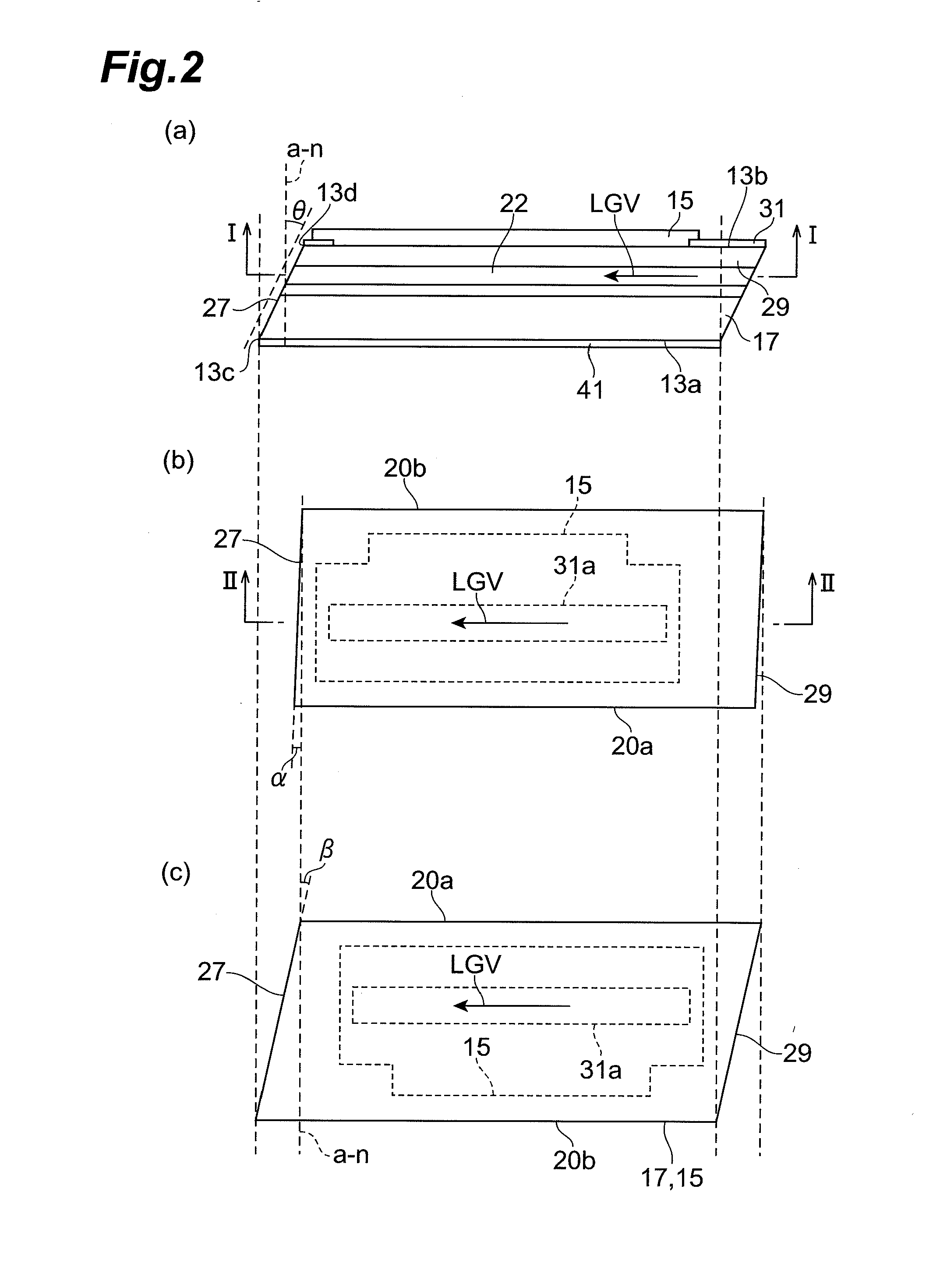
[0164]In Example 2, the plural epitaxial films for the semiconductor laser are grown on the GaN substrate having the {20-21} plane. The end faces for the optical cavity are formed by the formation of scribed grooves and the press as described above. In order to find candidates for these end faces, plane orientations which make an angle near 90 degrees with the (20-21) plane and are different from the a-plane are obtained by calculation. With reference to FIG. 14, the following angles and plane orientations have angles near 90 degrees to the (20-21) plane.

Specific plane index,Angle to {20-21} plane.(−1016):92.46 degrees;(−1017):90.10 degrees;(−1018):88.29 degrees.


PUM

PropertyMeasurementUnit
angleaaaaaaaaaa
angleaaaaaaaaaa
angleaaaaaaaaaa

Abstract

A method of fabricating a group-III nitride semiconductor laser device includes: preparing a substrate of a hexagonal group-III nitride semiconductor, where the substrate has a semipolar primary surface; forming a substrate product having a laser structure, an anode electrode and a cathode electrode, where the laser structure includes the substrate and a semiconductor region, and where the semiconductor region is formed on the semipolar primary surface; scribing a first surface of the substrate product in part in a direction of the a-axis of the hexagonal group-III nitride semiconductor; and carrying out breakup of the substrate product by press against a second surface of the substrate product, to form another substrate product and a laser bar.

Description

BACKGROUND OF THE INVENTION[0001]1. Field of the Invention[0002]The present invention relates to a III-nitride semiconductor laser device, and a method of fabricating the III-nitride semiconductor laser device.[0003]2. Related Background Art[0004]Patent Literature 1 discloses a laser device. When a primary surface of a substrate is a face inclined at 28.1 degrees from a {0001} plane toward a direction equivalent to the [1-100] direction, a secondary cleaved facet is a {11-20} planes perpendicular to both of the primary surface and optical cavity faces, and the laser device is of a rectangular parallelepiped shape.[0005]Patent Literature 2 discloses a nitride semiconductor device. The back surface of the substrate is polished for cleavage to reduce the total thickness to about 100 μm. A dielectric multilayer film is deposited on cleaved facets.[0006]Patent Literature 3 discloses a nitride-based compound semiconductor device. The substrate used for the nitride-based compound semicondu...

Claims


Application Information

Patent Timeline
Patent Type & Authority Applications(United States)
IPC IPC(8): H01L21/18
CPCH01S5/0014H01S5/0202H01S5/028H01S5/1085H01S5/16H01S2301/14H01S5/320275H01S5/04254H01S5/2201H01S5/10H01S5/343H01S5/22
Inventor YOSHIZUMI, YUSUKETAKAGI, SHIMPEIIKEGAMI, TAKATOSHIUENO, MASAKIKATAYAMA, KOJI
Owner SUMITOMO ELECTRIC IND LTD
Why Eureka
Try Eureka