Semiconductor pressure sensor
- Summary
- Abstract
- Description
- Claims
- Application Information
AI Technical Summary
Benefits of technology
Problems solved by technology
Method used
Image

Examples
first embodiment
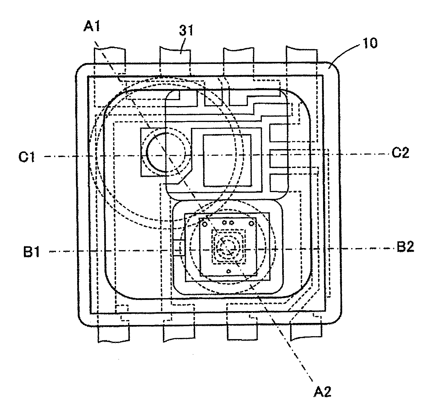
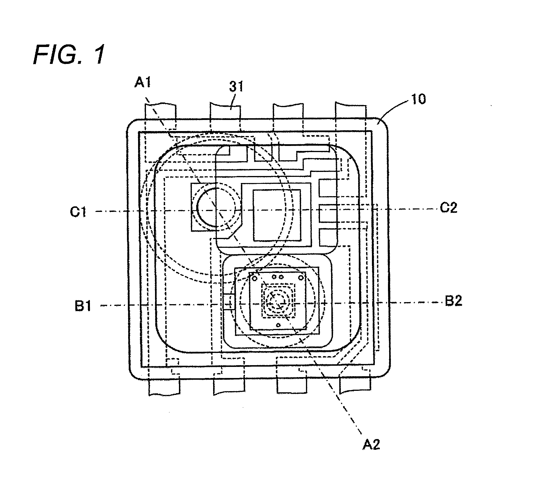
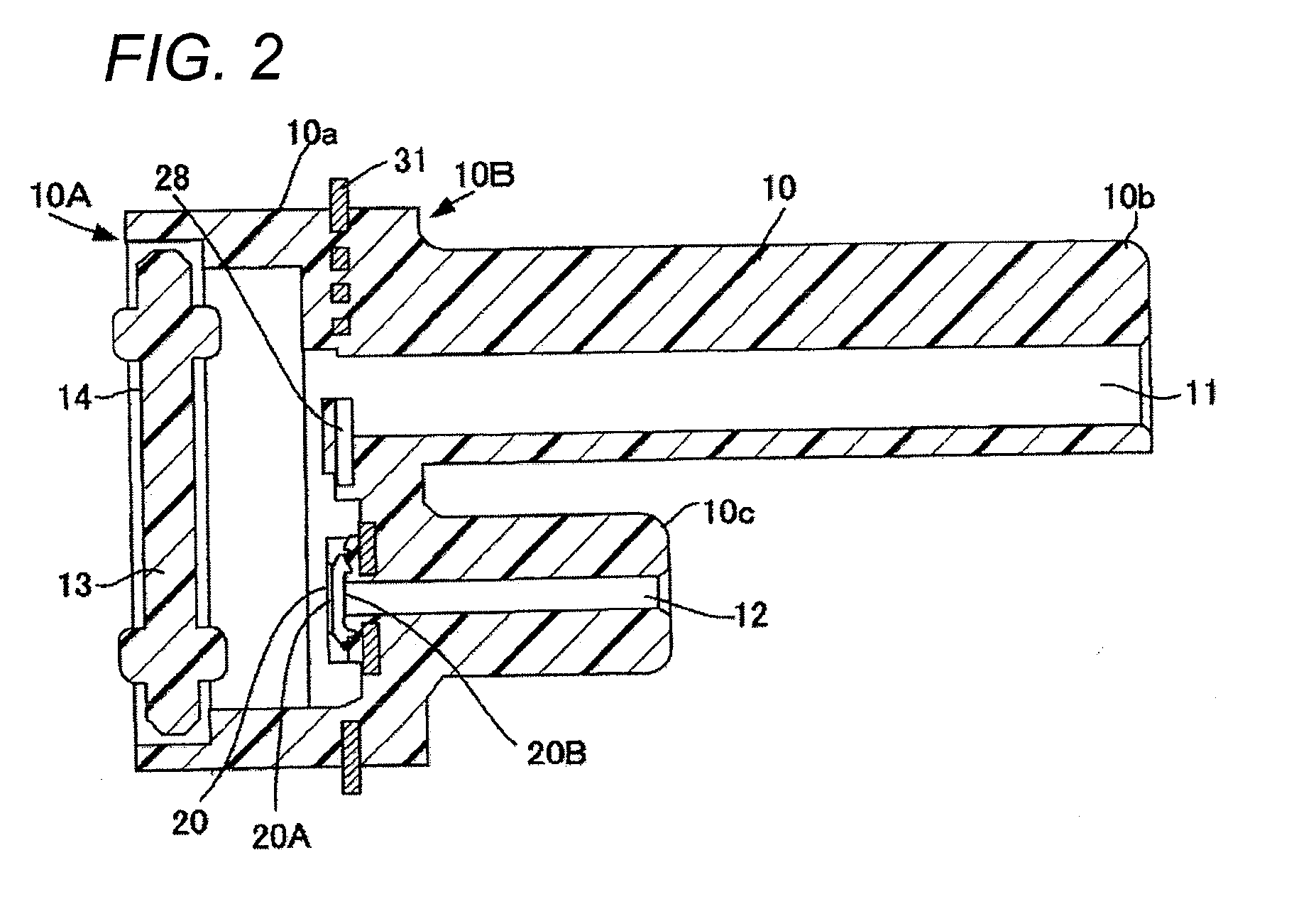
[0049]FIG. 1 is a top view of a semiconductor pressure sensor according to a first embodiment of the invention, FIG. 2 is a diagram illustrating a cross-section A1-A2 in FIG. 1, FIG. 3 is a diagram illustrating a cross-section B1-B2 in FIG. 1, FIG. 4 is a diagram illustrating a cross-section C1-C2 in FIG. 1, and FIGS. 5A and 5B are diagrams illustrating a pressure sensor chip which is used in the semiconductor pressure sensor, in which FIG. 5A is a top view and FIG. 5B is a cross-sectional view.
[0050]In the semiconductor pressure sensor according to the first embodiment of the invention, a pressure inlet port 11 and an atmosphere inlet port 12 are disposed on the same surface side of a case 10, the pressure inlet port 11 is communicated with the inside of the case 10, and a sensor chip 20 is disposed inside the case 10 at a position does not oppose the pressure inlet port 11. The case 10 is formed of a plastic resin, and includes the pressure inlet port 11 through which an external ...
second embodiment
[0070]Next, a semiconductor pressure sensor according to a second embodiment of the invention will be described.
[0071]FIG. 9 is a diagram illustrating the semiconductor pressure sensor according to the second embodiment of the invention. In the first embodiment, the atmosphere inlet port 12 is provided in the tubular atmospheric pressure inlet section 10c which is the extending section, but as shown as a modified example in FIG. 9, the atmosphere inlet port 12 may be directly formed on the case main body 10a. FIG. 9 shows the main portions only, but other elements except the atmospheric pressure inlet section 10c which is the extending section are formed in a similar way to the first embodiment. Reference numeral 20 represents a sensor chip of the semiconductor pressure sensor.
[0072]According to this configuration, it is possible to simplify the structure and to achieve a reduction in size.
third embodiment
[0073]Next, a semiconductor pressure sensor according to a third embodiment of the invention will be described.
[0074]In the first embodiment, the atmosphere inlet port 12 is provided in the atmospheric pressure inlet section 10c which is separately formed as the extending section on the case main body 10a, and the pressure inlet port 11 is provided in the pressure inlet section 10b which is separately formed as the extending section on the case main body 10a. On the other hand, in the present embodiment, as a modified example, the atmosphere inlet port 12 and the pressure inlet port 11 are directly formed in a single inlet section.
[0075]FIG. 10 is a perspective view illustrating the semiconductor pressure sensor according to the third embodiment of the invention.
[0076]The pressure inlet section 10b and the atmospheric pressure inlet section 10c are integrally formed, and the atmosphere inlet port 12 is perforated through the tubular wall of the atmospheric pressure inlet section 10c...
PUM
 Abstract
Description
Claims
Application Information
 - R&D
- Intellectual Property
- Life Sciences
- Materials
- Tech Scout
- Unparalleled Data Quality
- Higher Quality Content
- 60% Fewer Hallucinations
Browse by: Latest US Patents, China's latest patents, Technical Efficacy Thesaurus, Application Domain, Technology Topic, Popular Technical Reports.
© 2025 PatSnap. All rights reserved.Legal|Privacy policy|Modern Slavery Act Transparency Statement|Sitemap|About US| Contact US: help@patsnap.com