Plasma display panel

a technology of display panel and plasma, which is applied in the direction of address electrodes, static indicating devices, instruments, etc., can solve the problems of increasing the difficulty of fabricating discharge cells accurately over the whole surface of such a pdp, affecting the dimensional accuracy of the electrode, and affecting the discharging of many unstable factors, etc., to achieve stable writing, high definition, and large size

Inactive Publication Date: 2012-06-14
PANASONIC CORP
View PDF3 Cites 3 Cited by
  • Summary
  • Abstract
  • Description
  • Claims
  • Application Information

AI Technical Summary

Benefits of technology

[0007]The present invention is intended to provide a PDP which is large in size and has high definition but permits stable writing electric discharging over the whole surface of the display screen while suppressing increases in power consumption. A PDP according to the present invention has a first substrate, plural pairs of display electrodes, a second substrate, and plural data electrodes. The display electrodes are made up of scanning electrodes and sustain electrodes arranged parallel to each other on the first substrate. The second substrate is disposed opposite to the first substrate. A discharge space is formed between the first substrate and second substrate. The data electrodes are arranged on the second substrate in a direction perpendicular to the display electrodes. The data electrodes are wider in peripheral portions of the second substrate than in a central portion of the second substrate. Because of this configuration, even when a PDP is large in size and has high definition, it can suppress increases in power consumption. As a result, the PDP permitting stable writing electric discharging over the whole display screen can be obtained.

Problems solved by technology

However, the writing discharging involves many unstable factors.
One of the factors is that the discharging is easily affected by the dimensional accuracy of the electrodes.
It has become more difficult to fabricate discharge cells accurately over the whole surface of such a PDP.
However, the application of the shape of the data electrodes increases the power consumption.
If the shape of the data electrodes is designed in such a way that the power consumption is not increased, electric discharging is affected by the dimensional accuracy of the electrodes and thus is unstable.
With the shape of the data electrode relying on the related art technique in this way, it is difficult to accomplish both stability of electric discharging and suppression of power consumption.

Method used


Image

  • Plasma display panel
  • Plasma display panel
  • Plasma display panel

Examples


embodiment 1

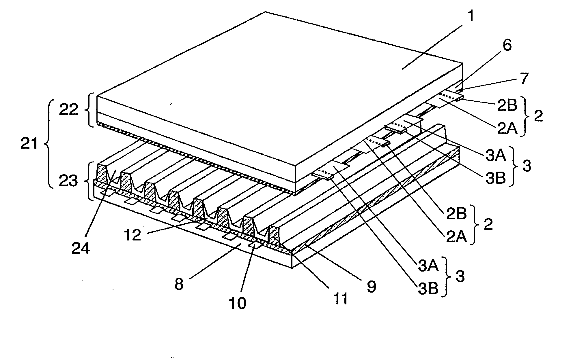
[0018]FIG. 1 is an exploded perspective view showing a structure of a plasma display panel according to the embodiment 1 of the present invention. Transparent electrodes 2A forming scanning electrodes 2 acting as display electrodes and transparent electrodes 3A forming sustain electrodes 3 are formed on front glass substrate (hereinafter referred to as “substrate”) 1 that is a first substrate. Auxiliary electrodes 2B and 3B are formed on electrodes 2A and 3A, respectively. That is, each scanning electrode 2 is made up of transparent electrode 2A and auxiliary electrode 2B. Each sustain electrode 3 is made up of transparent electrode 3A and auxiliary electrode 3B. Scanning electrodes 2 and sustain electrodes 3 are formed substantially parallel to each other and alternately.

[0019]Dielectric layer 6 is formed over substrate 1 so as to cover transparent electrodes 2A, 3A and auxiliary electrodes 2B, 3B. Dielectric layer 6 can be formed, for example, by applying glass paste by a die coat...

embodiment 2

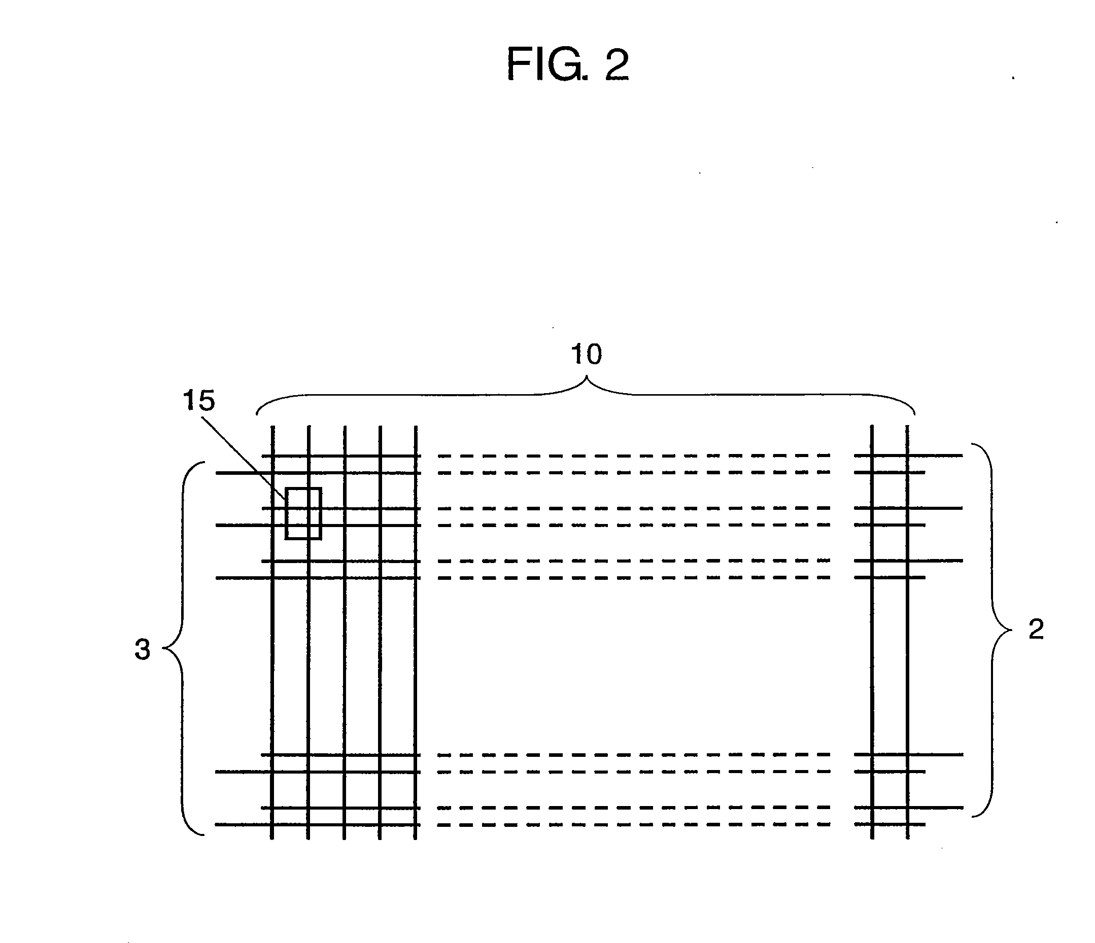
[0040]FIG. 7A is a plan view showing the shape of data electrodes of a plasma display panel according to embodiment 2 of the present invention. The great difference of the present embodiment with the embodiment 1 is that data electrodes arranged in peripheral portions of substrate 8 (plasma display panel) is wider than data electrodes arranged in the central portion of substrate 8. Since the embodiment 2 is similar to the embodiment 1 in other fundamental structures, its detailed description is omitted.

[0041]As shown in FIG. 7A, data electrodes 10E and 10F are mounted such that their width increases gradually from a central portion of substrate 8 toward left and right peripheral portions. That is, the width of the plural data electrodes continuously increases toward the peripheral portions of substrate 8 from the central portion of substrate 8. The discharging characteristics of the discharge cells are made to vary gradually by designing the panel in this way. Therefore, deteriorati...


PUM


Abstract

A plasma display panel has a first substrate, plural pairs of display electrodes, a second substrate, and plural data electrodes. Each pair of the display electrodes is made up of a scanning electrode and a sustain electrode which are arranged parallel to each other on the first substrate. The second substrate is disposed opposite to the first substrate. A discharge space is formed between the first substrate and second substrate. The data electrodes are arranged in a direction perpendicular to the display electrodes on the second substrate. The data electrode is wider in peripheral portion of the second substrate than in a central portion of the second substrate.

Description

[0001]This application is a continuation of U.S. patent application Ser. No. 10 / 594,161, filed Sep. 26, 2006, the contents of which are incorporated herein by reference.TECHNICAL FIELD[0002]The present invention relates to a plasma display panel for use in a large-sized display device or the like.BACKGROUND ART[0003]An AC plane discharge panel that typifies a plasma display panel (hereinafter abbreviated as “PDP”) has a front plate and a back plate disposed opposite to each other. A number of discharge cells are formed between the front and back plates. Display electrodes, each consisting a pair of electrodes (i.e., a scanning electrode and a sustain electrode), are formed on a front glass substrate in plural pairs and parallel to each other in the front plate. A dielectric layer and a protective layer are formed over the display electrodes. The back plate has a back glass substrate on which plural parallel data electrodes are formed. A dielectric layer is formed over the data elect...

Claims


Application Information

Patent Timeline
Patent Type & Authority Applications(United States)
IPC IPC(8): G09G5/00G09G3/288G09G3/291G09G3/296G09G3/298H01J11/12H01J11/22H01J11/24H01J11/26H01J11/34H01J11/46
CPCH01J2211/265H01J11/26
Inventor MURAKOSO, TOMOHIROOGAWA, KENJIANDO, TORUUEDA, KENTAROKOSHIO, YOHEIMURAI, RYUICHI
Owner PANASONIC CORP
Why Eureka
Try Eureka