Crystal oscillator and method of manufacturing the same

a crystal oscillator and crystal technology, applied in the field of crystal oscillators, can solve the problems of significantly increasing manufacturing costs, frequency changes, and methods that are not necessarily optimal, and achieve the effect of preventing the reduction of productivity

Inactive Publication Date: 2012-06-21
NIHON DEMPA KOGYO CO LTD
View PDF2 Cites 2 Cited by
  • Summary
  • Abstract
  • Description
  • Claims
  • Application Information

AI Technical Summary

Benefits of technology

[0015]It is an object of the present invention to provide a crystal oscillator that is not large scale, is not accompanied by significant increase in cost, has a small change in characteristics in a case of application of ionizing radiation such as X-ray application, and can maintain a constant oscillation frequency.
[0016]It is another object of the present invention to provide a method of manufacturing a crystal oscillator that is not large scale, is not accompanied by significant increase in cost, has a small change in characteristics in a case of application of ionizing radiation such as X-ray application, and can maintain a constant oscillation frequency.
[0018]In the crystal oscillator based on the present invention, ionizing radiation to be incident on the circuit formation plane into the IC chip is absorbed by the metal cover. Ionizing radiation to be incident on the main surface other than the circuit formation plane of the IC chip into this IC chip is absorbed by the radiation protective film. Accordingly, in this crystal oscillator, even in a case of application of radiation, the radiation does not adversely affect the electronic circuit in the IC chip. This allows change in characteristics of the crystal oscillator to be reduced, thereby enabling a constant oscillation frequency to be maintained.
[0020]This manufacturing method allows the radiation protective film corresponding to a plurality of IC chips to be formed at one time, thereby preventing reduction in productivity accompanied by providing the radiation protective film.

Problems solved by technology

Accordingly, even X-ray application in low intensity X-ray screening can cause a problem of frequency change owing to the application of radiation.
However, these methods are for high energy or high dose radiation, and have a large-scale configuration and significantly increase manufacturing cost.
These methods are not necessarily optimal as measures against low intensity X-ray application in airport security screening and the like.

Method used


Image

  • Crystal oscillator and method of manufacturing the same
  • Crystal oscillator and method of manufacturing the same
  • Crystal oscillator and method of manufacturing the same

Examples


Embodiment Construction

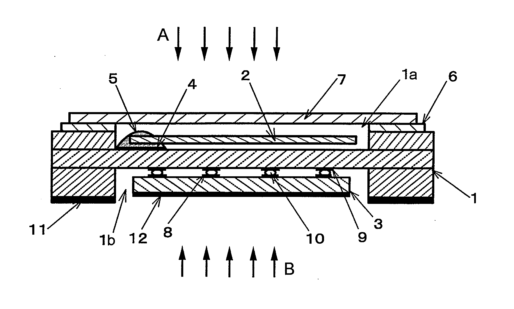
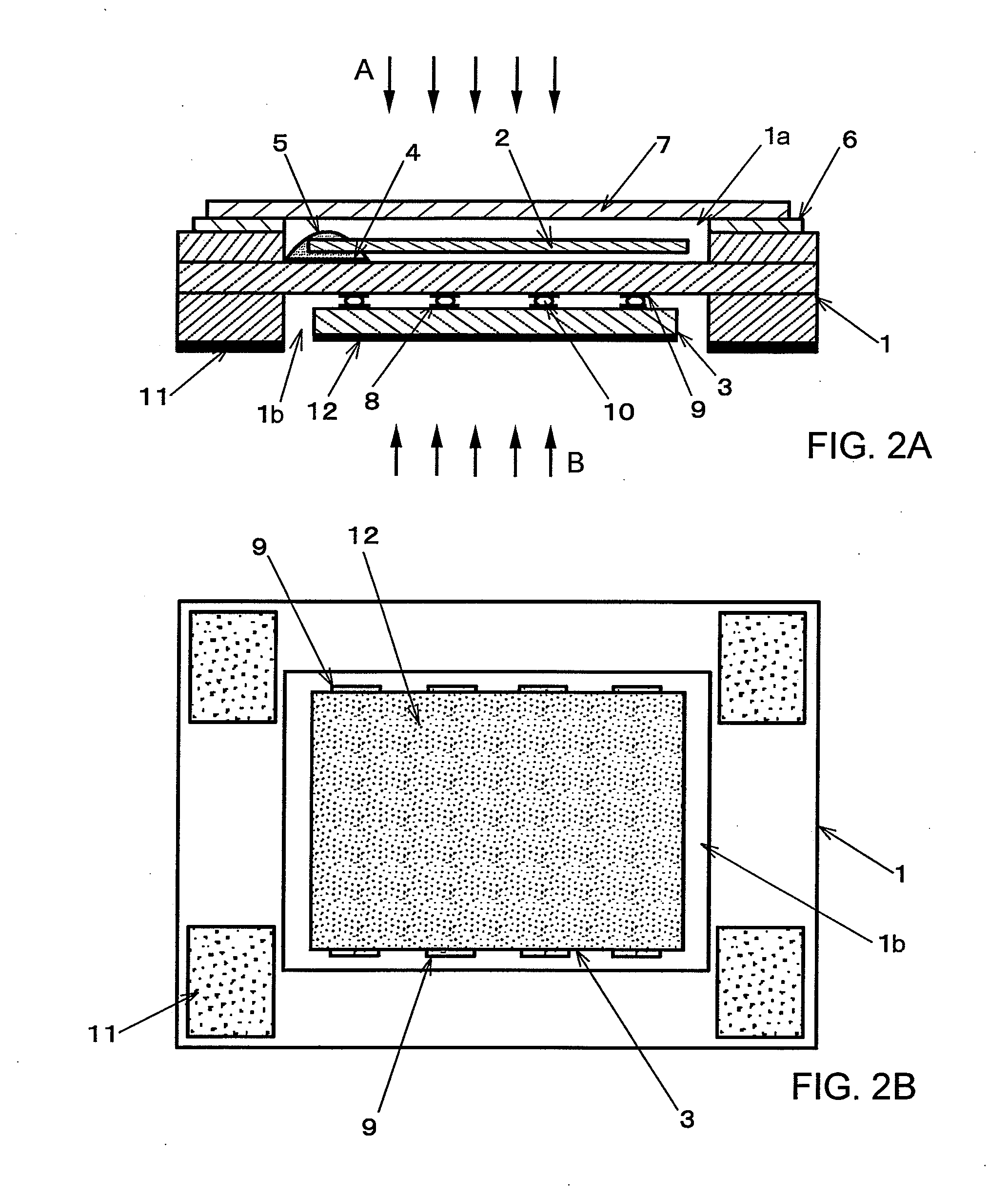
[0025]In FIGS. 2A and 2B showing a crystal oscillator according to an embodiment of the present invention, parts and constituents identical to those in FIGS. 1A and 1B are assigned with identical reference numerals, and description thereof is simplified or omitted.

[0026]The crystal oscillator of the present embodiment shown in FIGS. 2A and 2B has a surface mount configuration as with that shown in FIGS. 1A and 1B, and employs container body 1 where recesses 1a and 1b are formed on both respective main surfaces. Crystal blank 2 is housed in one recess 1a, and IC chip 3 is housed in other recess 1b. The crystal oscillator has a shape of a flat and substantially rectangular parallelepiped as a whole. The container body is made of, for example, a laminated ceramic. Mounting electrodes 11 used for surface-mounting the crystal oscillator on a circuit board or the like are provided on respective four corners of the end surface surrounding recess 1b. Crystal blank 2 is an AT-cut quartz crys...


PUM


Abstract

A crystal oscillator with improved tolerance to radiation such as X-rays includes: a container body; a quartz crystal blank accommodated in a first recess formed on one main surface of the container body and hermetically encapsulated in the first recess by a metal cover; and an IC chip that integrates electronic circuits including at least an oscillator circuit using the crystal blank and is accommodated in the second recess formed on the other main surface of the container body. The IC chip is fixed to the bottom surface of the second recess by flip-chip bonding such that a circuit formation plane of the IC chip is opposed to the bottom surface of the second recess. A radiation protective film is formed on the main surface other than the circuit formation plane of the IC chip.

Description

BACKGROUND OF THE INVENTION[0001]1. Field of the Invention[0002]The present invention relates to a quartz crystal oscillator that packages a quartz crystal blank and an IC (integrated circuit) chip, which integrates an oscillator circuit using the crystal blank, into a container having a recess in each of both main surfaces. In particular, the present invention relates to a crystal oscillator with improved tolerance to radiation such as X-rays, and a method of manufacturing the same.[0003]2. Description of the Related Art[0004]The crystal oscillator configured by packaging the crystal blank and the IC chip integrating the oscillator circuit using the crystal blank into a container can easily adopt a configuration of a surface mount component, and is widely built-in as a reference source of frequency and time in a mobile electronic device, for example, typified by a mobile phone.[0005]There are various configurations housing the crystal blank and the IC chip in the crystal oscillator...

Claims


Application Information

Patent Timeline
Patent Type & Authority Applications(United States)
IPC IPC(8): H03B1/00H01L21/50
CPCH01L2224/16225H01L2924/15153H01L2924/1517H01L24/81H01L2924/1532H01L23/552H01L2924/00013H01L24/16H01L2924/14H01L2224/13099
Inventor ASAMURA, FUMIO
Owner NIHON DEMPA KOGYO CO LTD
Why Eureka
Try Eureka