
Wafer splitting apparatus and wafer splitting process

Inactive Publication Date: 2012-06-28
LEXTAR ELECTRONICS CORP
View PDF2 Cites 4 Cited by
  • Summary
  • Abstract
  • Description
  • Claims
  • Application Information

AI Technical Summary

Benefits of technology

[0007]The invention is directed to a wafer splitting apparatus capable of reducing the time required for splitting a wafer.
[0008]The invention is directed to a wafer splitting process which is more time-saving.
[0011]In light of the foregoing, the first surface of the splitting knife body in the present embodiment stretches over the chip regions of the wafer in all the extending directions of the first surface passing through the center of the first surface. Thus, the splitting knife body of the present embodiment is capable of splitting the chip regions on the wafer into a plurality of dice simultaneously so as to save the fabrication time of the dice efficiently. Accordingly, the fabrication cost of the dice in the embodiments of the invention can be reduced effectively.

Problems solved by technology

However, in conventional technology, splitting is time consuming as the process is usually performed cut by cut using a knife having a single knife edge.
When the size of the wafer is larger or the number of chip regions to be split is higher, the process further requires more time and higher machine fabrication cost.

Method used


Image

  • Wafer splitting apparatus and wafer splitting process
  • Wafer splitting apparatus and wafer splitting process
  • Wafer splitting apparatus and wafer splitting process

Examples


first embodiment

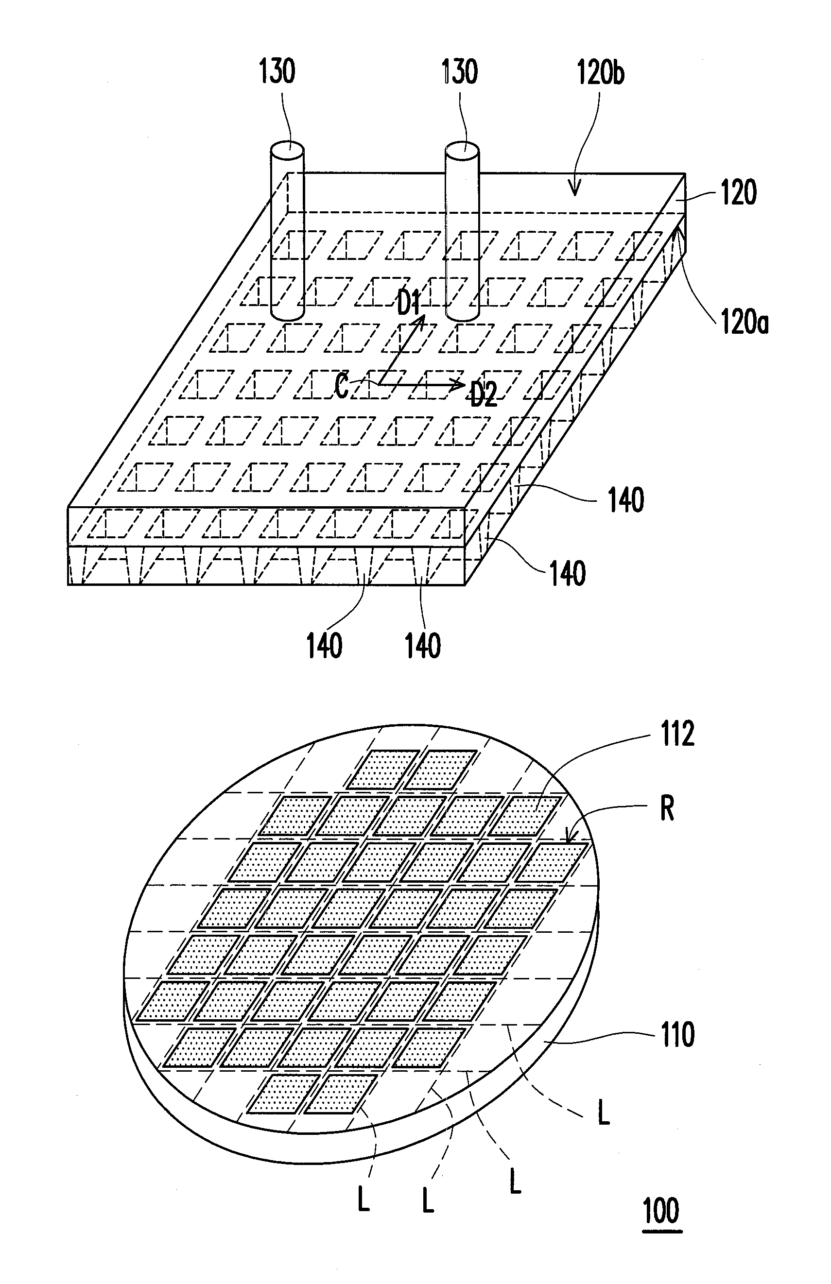
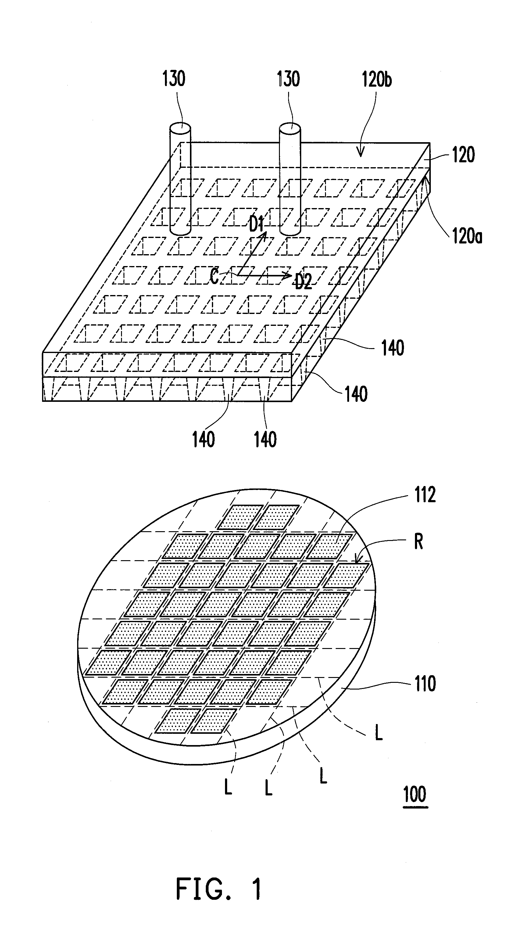
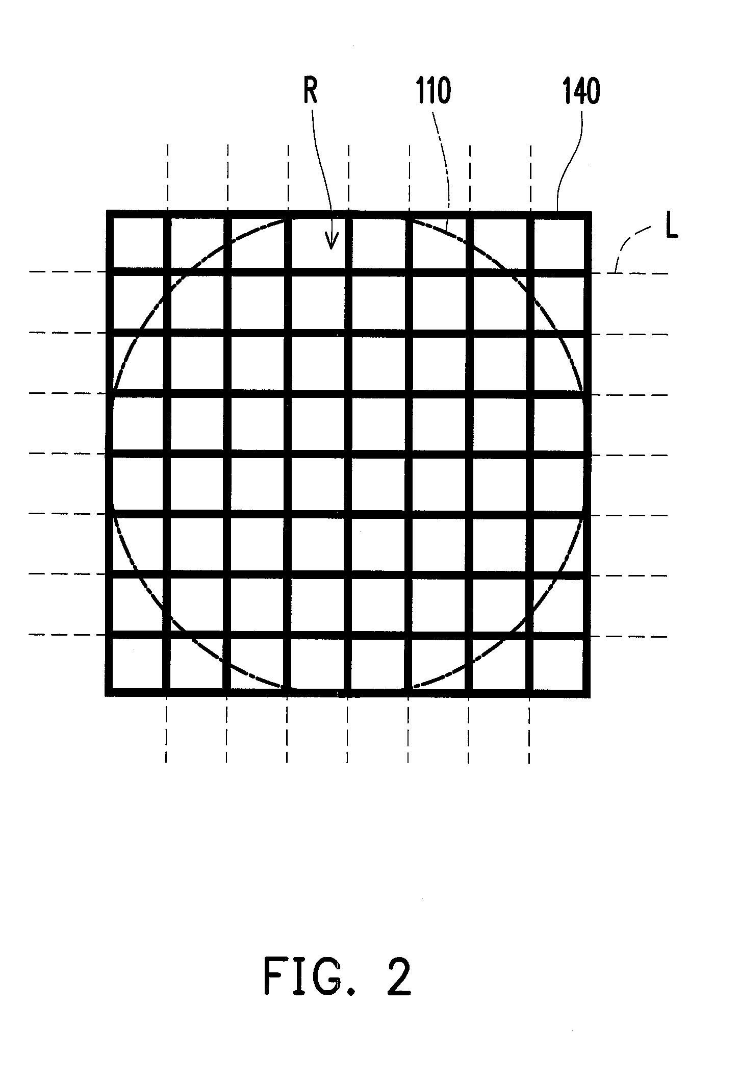
[0022]FIG. 1 illustrates a schematic diagram of a wafer splitting apparatus according to a first embodiment of the invention. Referring to FIG. 1, a wafer splitting apparatus 100 of the present embodiment is suitable for splitting a plurality of chip regions R in a wafer 110 into a plurality of independent dice 112. The wafer splitting apparatus 100 of the present embodiment includes a splitting knife body 120 and at least one vibrating hammer 130. In the present embodiment, the splitting knife body 120 is disposed at one side of the wafer 110 and has a first surface 120a facing the wafer 110. The first surface 120a stretches over a plurality of chip regions R of the wafer 110 in all extending directions of the first surface 120a passing through a center C of the first surface 120a.

[0023]For example, as shown in FIG. 1, the first surface 120a stretches over seven chip regions R of the wafer 110 in an extending direction D1 of the first surface 120a passing through the center C of t...

second embodiment

[0034]FIG. 9 illustrates a schematic diagram of a wafer splitting apparatus in a second embodiment of the invention. Referring to FIG. 9, a wafer splitting apparatus 100A in the present embodiment is similar to the wafer splitting apparatus 100 in the first embodiment, the similarities between the two are omitted hereinafter and the differences are illustrated below.

[0035]The wafer splitting apparatus 100A of the present embodiment is suitable for splitting a plurality of chip regions R in a wafer 110 into a plurality of independent dice 112. The wafer splitting apparatus 100A of the present embodiment includes a splitting knife body 120 and at least one vibrating hammer 130. The splitting knife body 120 of this embodiment is disposed at one side of the wafer 110 and has a first surface 120a facing the wafer 110. The first surface 120a stretches over a plurality of chip regions R of the wafer 110 in all extending directions of the first surface 120a passing through a center of the f...


PUM

PropertyMeasurementUnit
Forceaaaaaaaaaa

Abstract

A wafer splitting apparatus suitable for splitting a plurality of chip regions of a wafer into a plurality of independent dice is provided. The wafer splitting apparatus includes a splitting knife body and at least a vibrating hammer. The splitting knife body is disposed at one side of the wafer, and has a first surface facing the wafer. The first surface stretches over a plurality of chip regions in all extending directions of the first surface passing through a center of the first surface. The splitting knife body is disposed between the wafer and the vibrating hammer, and the vibrating hammer is suitable for knocking the splitting knife body in a direction toward the wafer to make the splitting knife body move toward the wafer, so as to split the chip regions of the wafer into a plurality of independent dice. A wafer splitting process is also provided.

Description

CROSS-REFERENCE TO RELATED APPLICATION[0001]This application claims the priority benefit of Taiwan application serial no. 99146138, filed Dec. 27, 2010. The entirety of the above-mentioned patent application is hereby incorporated by reference herein and made a part of this specification.BACKGROUND OF THE INVENTION[0002]1. Field of the Invention[0003]The invention relates to a wafer splitting apparatus and a wafer splitting process and more particularly to a wafer splitting apparatus and a wafer splitting process capable of reducing process time.[0004]2. Description of Related Art[0005]Light emitting diodes (LEDs) are semiconductor devices. Light emitting chips are mainly fabricated using compounds of group III-V elements, for example, gallium phosphide (GaP), gallium nitride (GaN) or gallium arsenide (GaAs). Moreover, LEDs emit light by converting electric energy into light energy. In details, currents are applied to compound semiconductors of LEDs so as to release energy in the fo...

Claims


Application Information

Patent Timeline
IPC IPC(8): B28D5/04
CPCB28D5/0023H01L33/0095B28D5/0041
Inventor WENG, CHIEN-SENXING, MENG-YENGYU, WEI-CHANGCHEN, CHIH-SHENGCHANG, YU-CHING
Owner LEXTAR ELECTRONICS CORP
Learn More