Laminate type electronic component and manufacturing method therefor

a technology of electronic components and manufacturing methods, applied in the direction of fixed capacitor details, generators/motors, fixed capacitors, etc., can solve the problems of inability to adopt batch treatment, inability to enjoy the advantages of batch treatment, and inability to reduce the effective volume of ensuring capacitance, etc., to achieve the effect of easy prevention of damag

Active Publication Date: 2012-06-28
MURATA MFG CO LTD
View PDF1 Cites 9 Cited by
  • Summary
  • Abstract
  • Description
  • Claims
  • Application Information

AI Technical Summary

Benefits of technology

[0011]Preferred embodiments of the present invention provide a method for manufacturing a laminate type electronic component, which makes it possible to apply a batch treatment, and makes it possible to efficiently form a plating film to serve as an external electrode in a specific position.
[0023]According to a preferred embodiment of the present invention, the conductive particles are preferably arranged in island-shaped configurations, and a discontinuous film of the conductive particles is thus formed over the entire surface of the component main body. While this discontinuous film is a halfway conductor film in a way, the combination of the discontinuous conductor film with electrolytic plating allows plating growth to be developed in the region with the respective exposed ends of the plurality of internal electrodes gathered at the surface of the component main body, and in the vicinity of the region, while plating growth is not allowed to be developed in the other region. Accordingly, even when a batch treatment such as barrel plating is carried out, a plating film can be formed only in a region where an external electrode is desired to be formed.
[0024]In addition, in a preferred embodiment of the present invention, electrolytic plating is applied to the formation of the plating film, and therefore it is easy to prevent damage caused by the plating solution to the laminated body, as compared with a case of electroless plating being used.

Problems solved by technology

Therefore, in order to limit the dimensions of the laminate type electronic component up to certain specifications, there is undesirably a need to reduce the effective volume for ensuring a capacitance, because there is a need to ensure the volume for the paste electrode layers.
However, it is not possible to adopt the batch treatment simply in the masking-etching process to remove a specific section of the metal thin film.
Accordingly, after all, the method disclosed in Japanese Patent Application Laid-Open No. 63-104314 will not be able to enjoy the advantages of the batch treatment, such as the ability to efficiently treat a large number of chips of component main bodies.

Method used


Image

  • Laminate type electronic component and manufacturing method therefor
  • Laminate type electronic component and manufacturing method therefor
  • Laminate type electronic component and manufacturing method therefor

Examples


Embodiment Construction

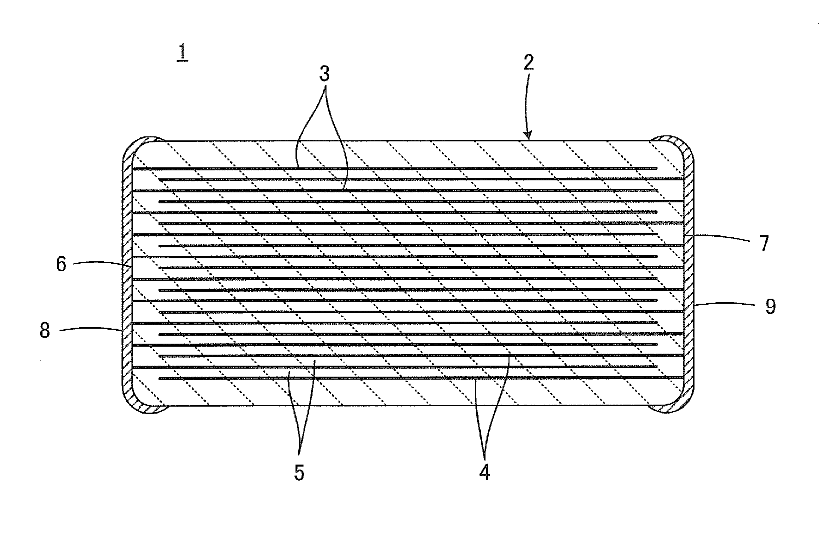
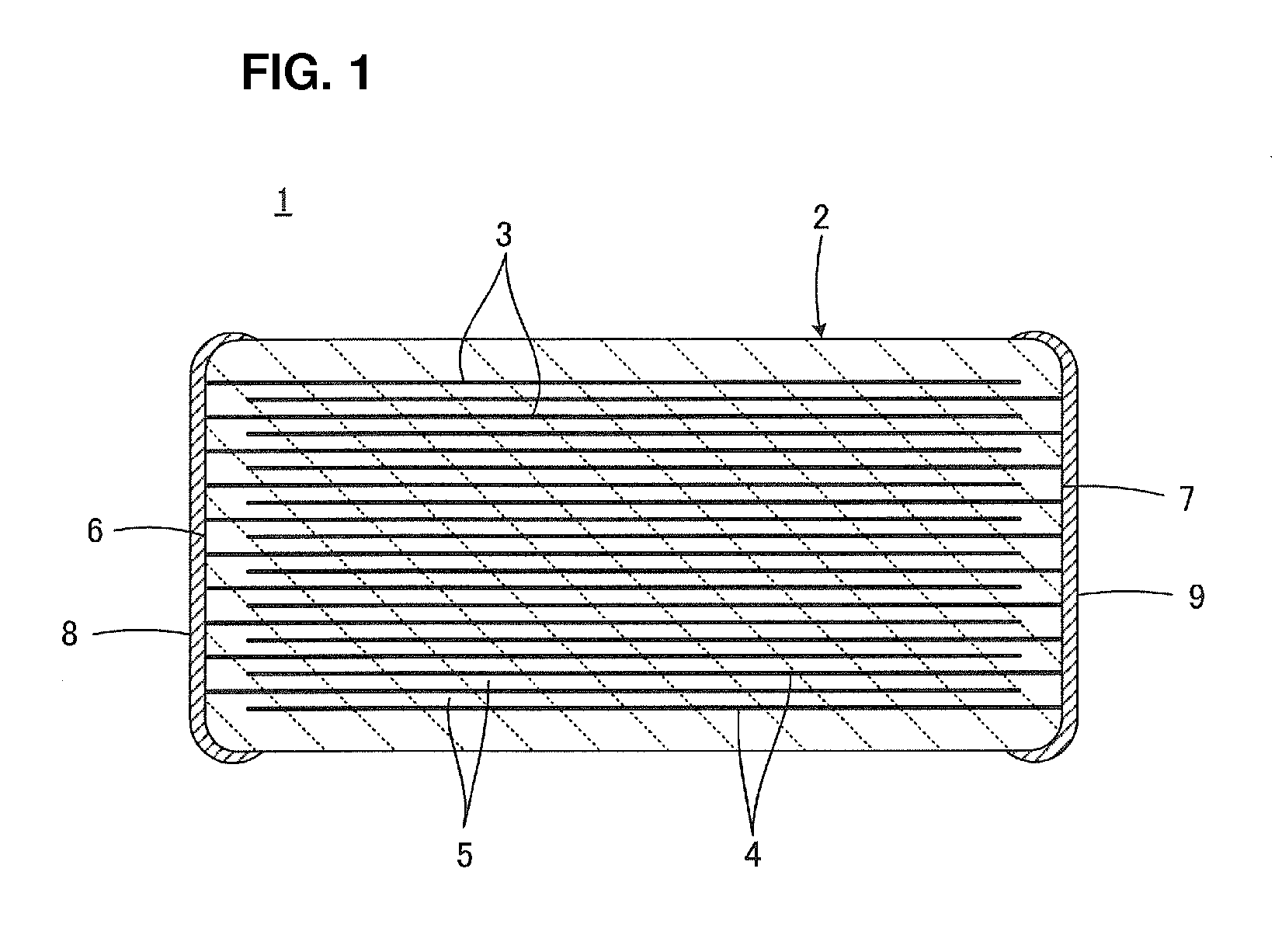
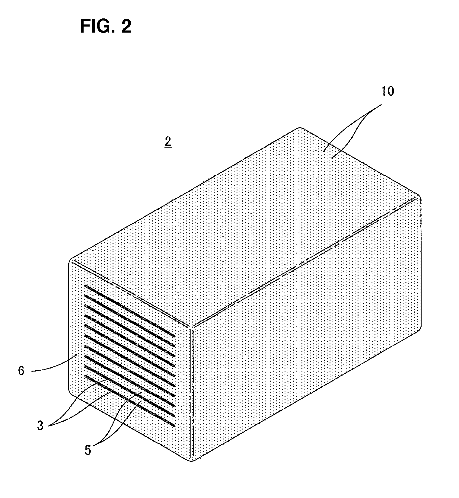
[0028]With reference to FIGS. 1 and 2, a laminate type electronic component will be described to which various preferred embodiments of the present invention are applied.

[0029]A laminate type electronic component 1 includes a component main body 2 which preferably has a stacked structure. The component main body 2 includes a plurality of internal electrodes 3 and 4 provided therein. More specifically, the component main body 2 includes a plurality of functional material layers 5 stacked, and a plurality of layered internal electrodes 3 and 4 arranged along the interfaces between the functional material layers 5. The internal electrodes 3 and the internal electrodes 4 are arranged alternately in the stacking direction. The internal electrodes 3 and 4 contain, for example, nickel as their main constituent.

[0030]When the laminate type electronic component 1 constitutes a laminated ceramic capacitor, the functional material layers 5 are preferably composed of a dielectric ceramic. It is...


PUM

PropertyMeasurementUnit
distanceaaaaaaaaaa
particle sizeaaaaaaaaaa
distanceaaaaaaaaaa

Abstract

In a method of manufacturing a laminate type electronic component, while the distance between adjacent exposed ends of a plurality of internal electrodes is adjusted preferably to be about 50 μm or less, a plurality of conductive particles composed of Pd, Pt, Cu, Au, or Ag are provided on the surface of a component main body. The conductive particles have an average particle size of about 0.1 nm to about 100 nm, which are distributed in island-shaped configurations over the entire surface of the component main body, while the average distance between the respective conductive particles is adjusted to fall within the range of about 10 nm to about 100 nm. The component main body is subjected to electrolytic plating such that plating growth develops in and around a region including the respective exposed ends of the plurality of internal electrodes.

Description

BACKGROUND OF THE INVENTION[0001]1. Field of the Invention[0002]The present invention relates to a laminate type electronic component and a method for manufacturing the laminate type electronic component, and more particularly, relates to a laminate type electronic component with an external electrode formed directly by plating in such a way that the external electrode is at least partially connected electrically to a plurality of internal electrodes, and a method for manufacturing the laminate type electronic component.[0003]2. Description of the Related Art[0004]Laminate type electronic components typified by laminated ceramic capacitors are, in general, provided with a component main body which has a stacked structure including, for example, a plurality of stacked functional material layers composed of a dielectric ceramic, and a plurality of layered internal electrodes formed along the interfaces between the functional material layers. The respective ends of the plurality of int...

Claims


Application Information

Patent Timeline
Patent Type & Authority Applications(United States)
IPC IPC(8): H01L41/00H01C7/13H01F5/00H01G4/12C25D15/00H01C7/10B82Y99/00H01G4/232H01G4/30
CPCH01G4/005H01G4/008H01G4/12Y02E60/13H01G4/30H01G11/34H01G4/228
Inventor MOTOKI, AKIHIROOGAWA, MAKOTO
Owner MURATA MFG CO LTD
Why Eureka
Try Eureka