Method of making a copper wire bond package

Inactive Publication Date: 2012-06-28
ALPHA & OMEGA SEMICON INC
View PDF4 Cites 17 Cited by
  • Summary
  • Abstract
  • Description
  • Claims
  • Application Information

AI Technical Summary

Benefits of technology

[0005]The present invention aims at providing an improved lead frame and a corresponding method for making a copper wire bond package by increasing the lead

Problems solved by technology

The mutually separated die pads are connected to the lead frame with tie bars in a few locations that may not provide adequate support in

Method used


Image

  • Method of making a copper wire bond package
  • Method of making a copper wire bond package
  • Method of making a copper wire bond package

Examples


Embodiment Construction

[0020]The present invention is detailed in combination with the drawings and descriptions of the preferred embodiments as follows.

[0021]The package structure and its making method provided by the present invention are applicable to various types of semiconductor chips, including FET chips and IC control chips, etc. In the detailed description of the embodiments below, MOSFET chips are taken as example to explain the advantages and favorable effects of the present invention. However, it shall be noted that the description and embodiments do not constitute limitations to the protection scope of the present invention.

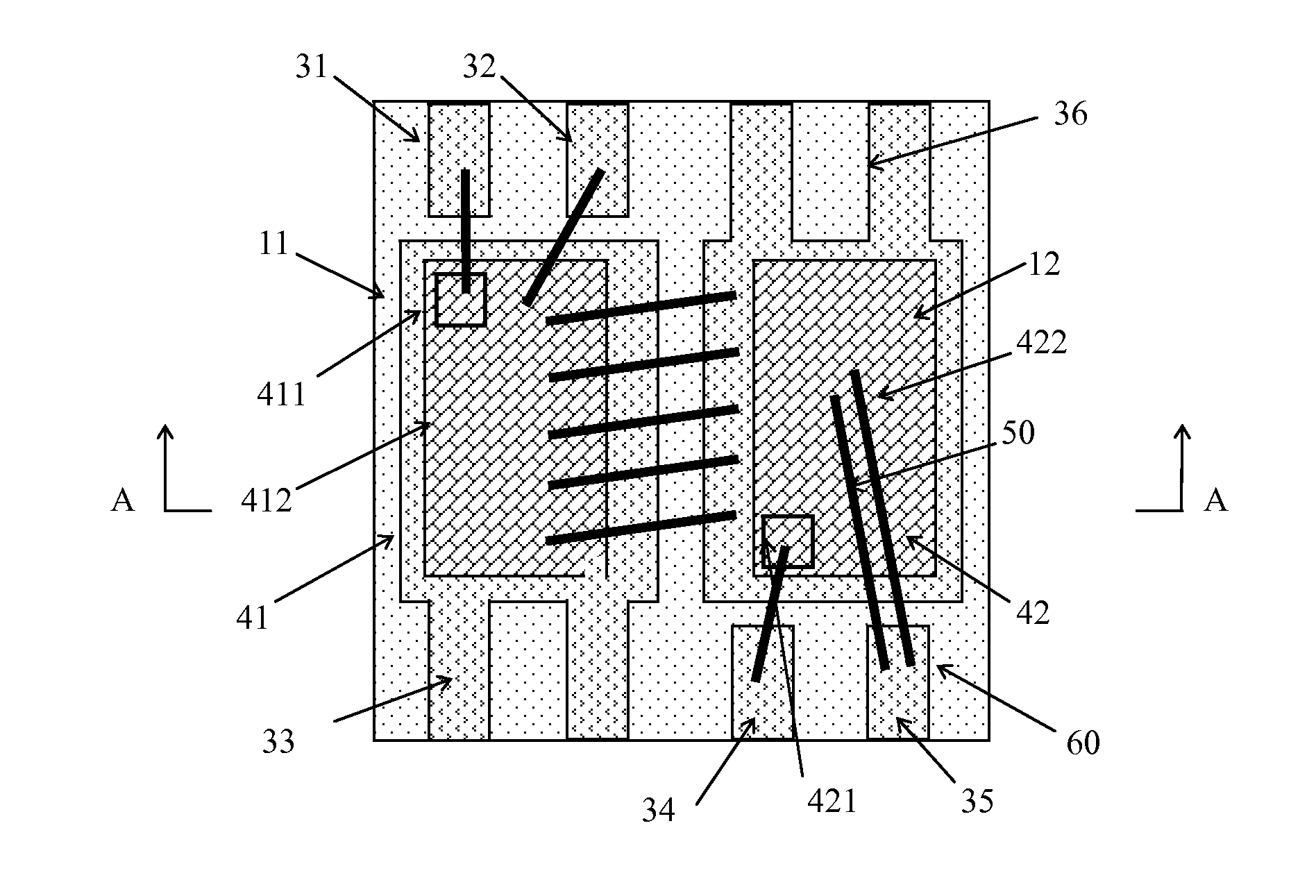
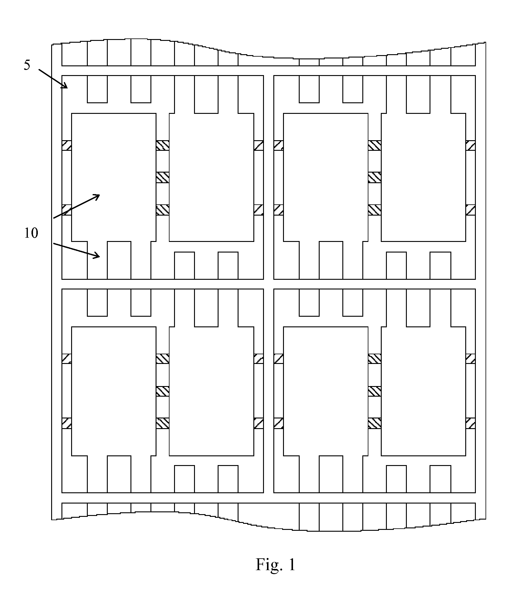
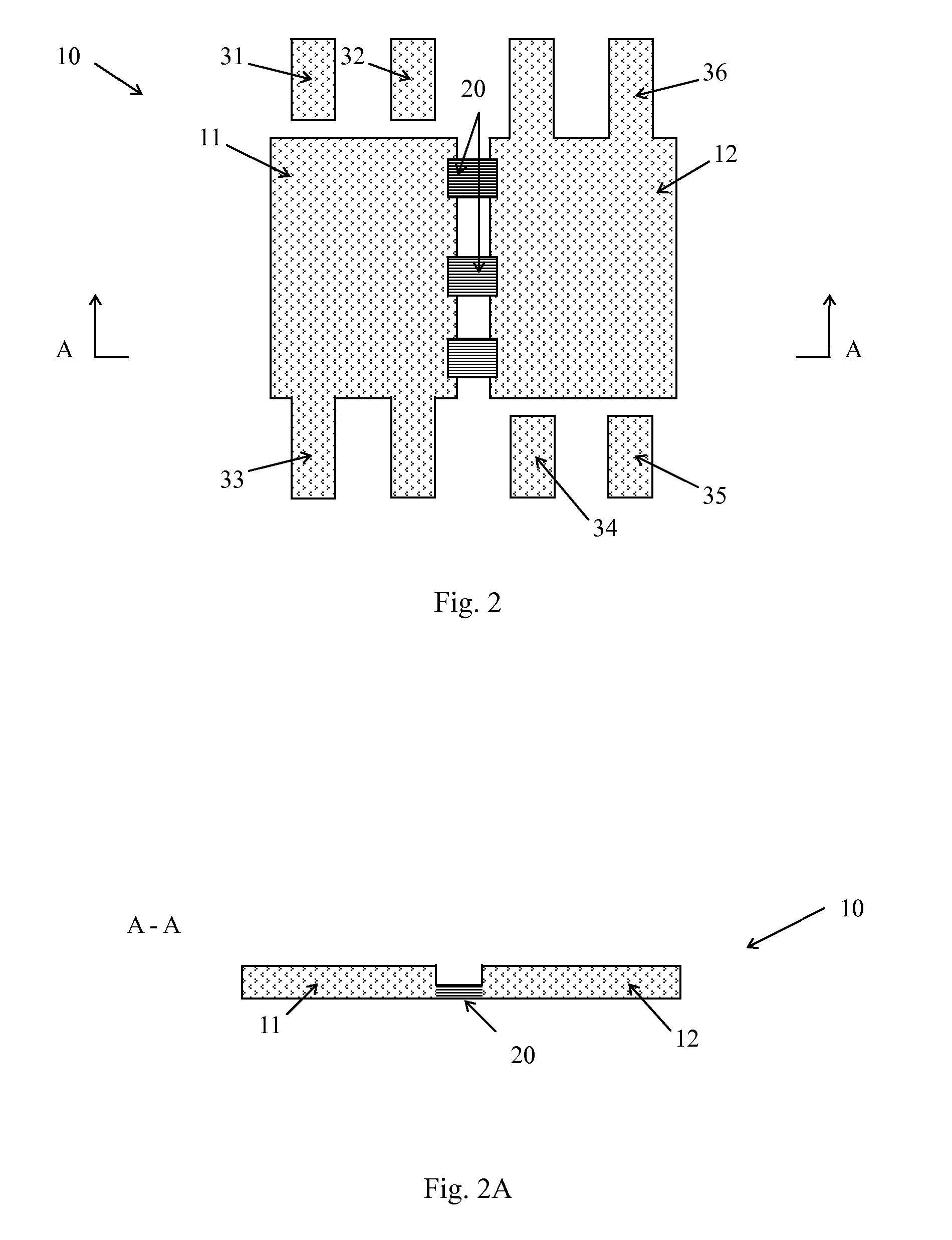
[0022]FIG. 1 is a diagram of a lead frame array 5 comprising a plurality of lead frame units 10 according to current invention. FIG. 2 is a top view of the structure of one lead frame unit 10 and FIG. 2A is a cross sectional view of the lead frame unit along A-A line. Each lead frame unit 10 comprises a first die pad 11 and a second die pad 12 on the lead frame 10 for moun...


PUM


Abstract

A method for making a wire bond package comprising the step of providing a lead frame array comprising a plurality of lead frame units therein, each lead frame unit comprises a first die pad and a second die pad each having a plurality of tie bars connected to the lead frame array, a plurality of reinforced bars interconnecting the first and second die pads; the reinforced bars are removed after molding compound encapsulation.

Description

BACKGROUND OF THE INVENTION[0001]1. Technical Field[0002]The present invention relates to a method of making a semiconductor package, and more especially, to a method of making multi-chip copper wire bonding semiconductor package.[0003]2. Description of Related Art[0004]A multi-chip semiconductor package usually requires a lead frame with more than one die pad to accommodate the multiple semiconductor chips. The die pads in a lead frame are mutually separated to maintain electrical isolation between different semiconductor chips, which is particular important for vertical semiconductor chips such as vertical metal oxide semiconductor field effect transistors (MOSFETs) where the drain electrode disposed on the bottom of MOSFET chip is electrically connected to the die pad. The mutually separated die pads are connected to the lead frame with tie bars in a few locations that may not provide adequate support in the wire bonding process, especially with the current trend to replace gold ...

Claims


Application Information

Patent Timeline
IPC IPC(8): H01L21/60H01L21/56
CPCH01L23/3107H01L2924/1306H01L23/4952H01L23/49562H01L23/49575H01L24/29H01L24/45H01L24/48H01L24/49H01L24/83H01L24/85H01L24/97H01L2224/32225H01L2224/45124H01L2224/45144H01L2224/45147H01L2224/48091H01L2224/48247H01L2224/49111H01L2224/73265H01L2224/92247H01L2224/97H01L2924/01013H01L2924/01029H01L2924/01079H01L2924/01082H01L2924/0781H01L23/49503H01L2924/01015H01L2224/83H01L2224/0603H01L2224/85H01L2924/13091H01L2924/01033H01L2224/32245H01L2924/00014H01L2924/00H01L2924/181H01L2224/05554H01L2924/00012
Inventor XUE, YAN XUNLU, JUNBHALLA, ANUP
Owner ALPHA & OMEGA SEMICON INC
Why Eureka
Try Eureka