Trench embedding method and film-forming apparatus

a film-forming apparatus and trench-based technology, applied in the direction of coatings, chemical vapor deposition coatings, metallic material coating processes, etc., can solve the problems of difficult or impossible to form a film serving as an oxidizing barrier in the trench

Active Publication Date: 2012-06-28
TOKYO ELECTRON LTD
View PDF7 Cites 369 Cited by
  • Summary
  • Abstract
  • Description
  • Claims
  • Application Information

AI Technical Summary

Problems solved by technology

However, if a trench is further miniaturized, it may be difficult or impossible to form a

Method used


Image

  • Trench embedding method and film-forming apparatus
  • Trench embedding method and film-forming apparatus
  • Trench embedding method and film-forming apparatus

Examples


Embodiment Construction

Embodiments for Carrying Out the Invention

[0026]An embodiment of the present invention achieved on the basis of the findings given above will now be described with reference to the accompanying drawings. In the following description, the constituent elements having substantially the same function and arrangement are denoted by the same reference numerals, and a repetitive description will be made only when necessary.

[0027](Embedding Method)

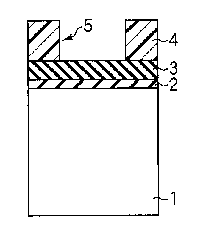
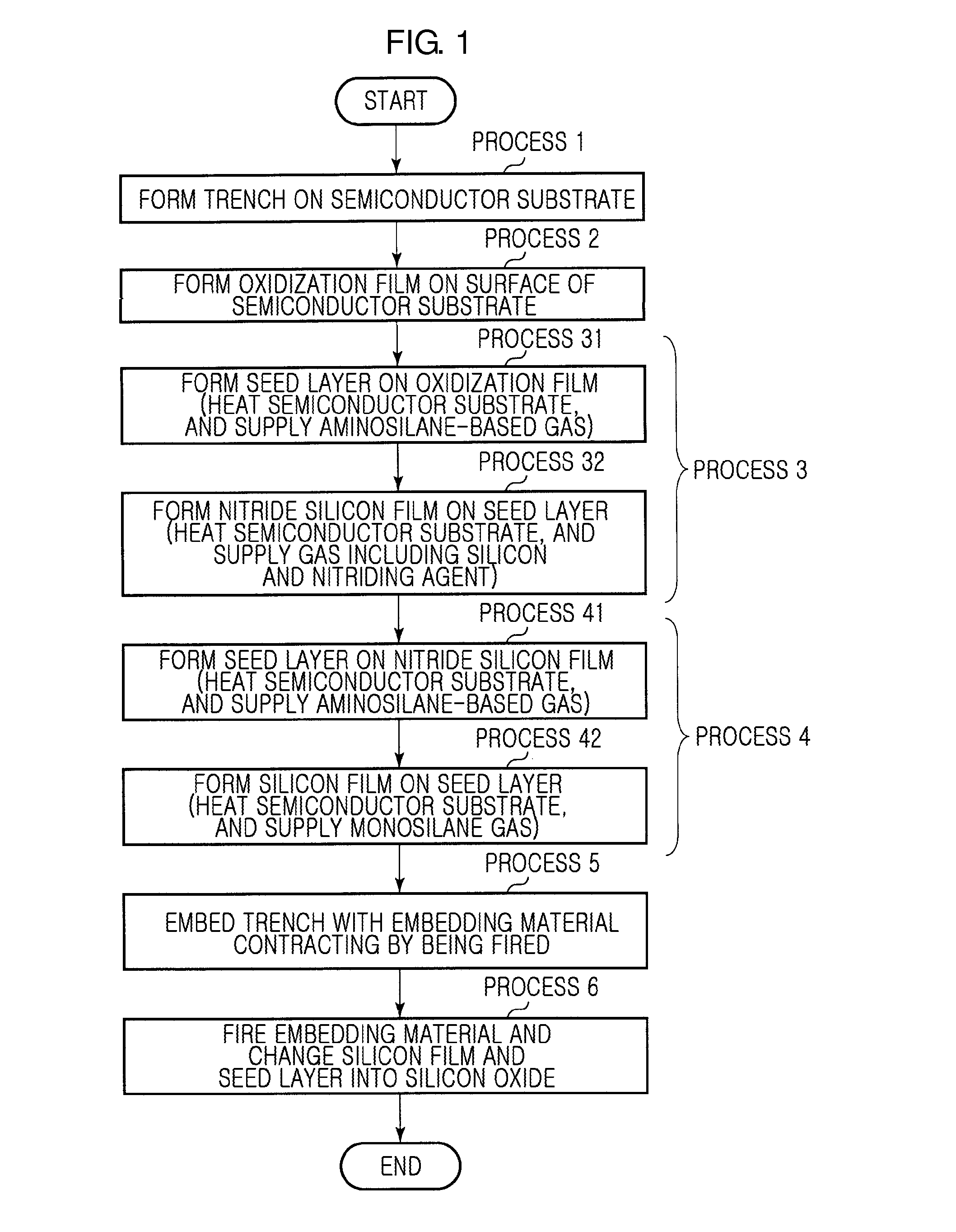
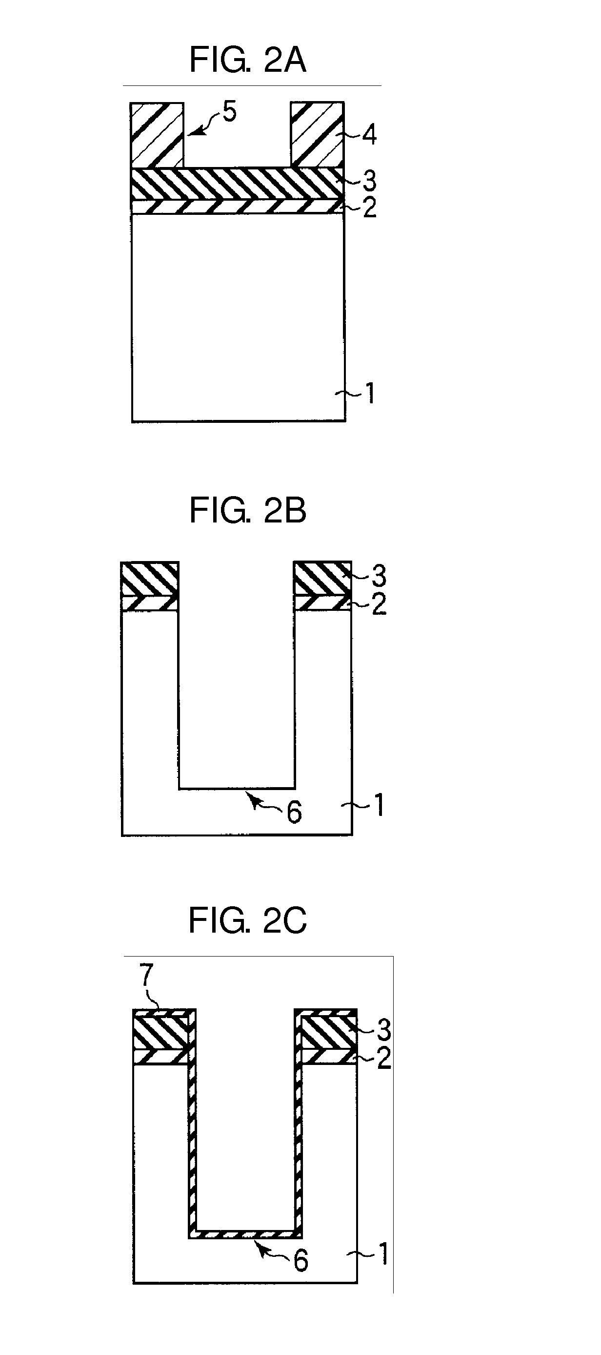
[0028]FIG. 1 is a flowchart showing a sequence of a trench embedding method according to an embodiment of the present invention. FIGS. 2A through 2I are cross-sectional views schematically showing states of a semiconductor substrate during the sequence shown in FIG. 1.

[0029]First, as shown in process 1 of FIG. 1, a trench is formed on the semiconductor substrate.

[0030]An example of forming the trench on the semiconductor substrate is as follows.

[0031]As shown in FIG. 2A, a surface of the semiconductor substrate, that is, a silicon substrate 1 in t...


PUM

PropertyMeasurementUnit
Thicknessaaaaaaaaaa
Thicknessaaaaaaaaaa
Areaaaaaaaaaaa

Abstract

A trench embedding method includes forming an oxidization barrier film on a trench; forming an expandable film on the oxidization barrier film; embedding an embedding material that contracts by being fired on the trench; and firing the embedding material, wherein the forming of the oxidization barrier film includes: forming a first seed layer on the trench by supplying an aminosilane-based gas; and forming a silicon nitride film on the first seed layer, wherein the forming of the expandable film includes: forming a second seed layer on the silicon nitride film by supplying an aminosilane-based gas; and forming a silicon film on the second seed layer.

Description

CROSS-REFERENCE TO RELATED PATENT APPLICATIONS[0001]This application claims the benefit of Japanese Patent Application No. 2010-290647, filed on Dec. 27, 2010 in the Japan Patent Office, the disclosure of which is incorporated herein in its entirety by reference.BACKGROUND OF THE INVENTION[0002]1. Field of the Invention[0003]The present invention relates to a trench embedding method and a film-forming apparatus.[0004]2. Description of the Related Art[0005]Semiconductor integrated circuit devices have a minute trench structure therein. A typical example of the minute trench structure is a STI (shallow trench isolation). An STI is a device isolation area for dividing active areas of a semiconductor device, and is formed by forming a minute trench on a silicon substrate and embedding an insulating material into the minute trench.[0006]For example, an SOD (spin-on dielectric), as disclosed in Patent Reference 1, is known as an embedded insulating material. In particular, an inorganic po...

Claims


Application Information

Patent Timeline
IPC IPC(8): H01L21/31C23C16/42
CPCH01L21/76227H01L21/76
Inventor WATANABE, MASAHISAOKADA, MITSUHIRO
Owner TOKYO ELECTRON LTD
Why Eureka
Try Eureka