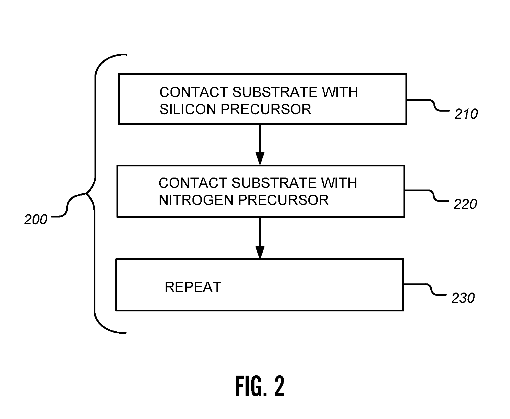
Deposition of SiN

a silicon nitride and low temperature technology, applied in the direction of coatings, chemical vapor deposition coatings, metallic material coating processes, etc., can solve the problems of affecting the production efficiency of silicon nitride films, the film deposited on the sidewalls of trenches or fins or other three-dimensional features displays inferior film properties as compared, and the structure such as these would not generally survive further processing

Active Publication Date: 2016-03-17
ASM IP HLDG BV
View PDF5 Cites 368 Cited by
  • Summary
  • Abstract
  • Description
  • Claims
  • Application Information

AI Technical Summary

Benefits of technology

[0033]The method of depositing the thin film may include removing excess reactants from the reaction space between the first plasma and the second plasma, and removing excess reactants from the reaction space between the second plasma and the third plasma. In some embodiments, removing excess reactants from the reaction space between the first plasma and the second plasma, and between the second plasma and the third plasma can each include flowing hydrogen gas. In some embodiments, removing excess reactants from the reaction space a first purge step between the first plasma and the second plasma can include ramping down a flow rate of nitrogen gas. In some embodiments, removing excess reactants from the reaction space between the second plasma and the third plasma includes flowing hydrogen gas and nitrogen gas. In some embodiments, the removing excess reactants from the reaction space between the second plasma and the third plasma includes ramping up a flow rate of nitrogen gas.

Problems solved by technology

Current PEALD silicon nitride processes in general suffer from anisotropic etch behavior when deposited on a three-dimensional structure, such as a trench structure.
In other words, the film deposited on the sidewalls of a trench or fin or another three dimensional feature display inferior film properties as compared to film on the top region of the feature.
Structures such as these would not generally survive further processing, such as in a FinFET spacer application.

Method used


Image

  • Deposition of SiN
  • Deposition of SiN
  • Deposition of SiN

Examples


example 1

[0295]Two examples of a cycle of silicon nitride film formation processes are provided below. Each process includes a combination of a PEALD silicon nitride deposition process with a nitrogen plasma treatment, and wet etch performance of silicon nitride films formed using each sequence is graphed in FIG. 9, as discussed below.

example a

[0296]A cycle of a silicon nitride film formation process included exposing a target substrate to plasma for a total of 18 seconds: exposing a target substrate for 2 seconds to a silicon precursor, followed by exposing the target substrate for 6 seconds to plasma generated for nitrogen precursors by nitrogen (N2) and hydrogen (H2) at a power of about 50 W, followed by exposing the target substrate for 6 seconds to a plasma generated by nitrogen (N2) and argon (Ar) for a nitrogen plasma treatment at a plasma power of about 200 W, and followed by exposing the target substrate for 6 seconds to the plasma generated from nitrogen (N2) and hydrogen (H2) at a plasma power of about 50 W (e.g., for providing —NH surface functional groups to the target substrate surface).

example b

[0297]A cycle of a silicon nitride film formation process included exposing a target substrate to plasma for a total of 30 seconds: exposing a target substrate for 2 seconds to a silicon precursor, followed by exposing the target substrate for 12 seconds to plasma generated for nitrogen precursors using nitrogen (N2) and hydrogen (H2) at a power of about 50 W, followed by exposing the target substrate for 6 seconds to a plasma generated by nitrogen (N2) and argon (Ar) for a nitrogen plasma treatment at a plasma power of about 200 W, and followed exposing the target substrate for 12 seconds to the plasma generated from nitrogen (N2) and hydrogen (H2) at a plasma power of about 50 W (e.g., for providing —NH surface functional groups to the target substrate surface).

[0298]Each of the example cycles were repeated for a number of times to obtain a desired silicon nitride film thickness and achieve a silicon nitride film having desired properties. A purge process prior to performing the n...


PUM

PropertyMeasurementUnit
etch rateaaaaaaaaaa
etch rateaaaaaaaaaa
poweraaaaaaaaaa

Abstract

Methods and precursors for forming silicon nitride films are provided. In some embodiments, silicon nitride can be deposited by atomic layer deposition (ALD), such as plasma enhanced ALD. In some embodiments, deposited silicon nitride can be treated with a plasma treatment. The plasma treatment can be a nitrogen plasma treatment. In some embodiments the silicon precursors for depositing the silicon nitride comprise an iodine ligand. The silicon nitride films may have a relatively uniform etch rate for both vertical and the horizontal portions when deposited onto three-dimensional structures such as FinFETS or other types of multiple gate FETs. In some embodiments, various silicon nitride films of the present disclosure have an etch rate of less than half the thermal oxide removal rate with diluted HF (0.5%). In some embodiments, a method for depositing silicon nitride films comprises a multi-step plasma treatment.

Description

REFERENCE TO RELATED APPLICATIONS[0001]The application claims the benefit of U.S. Provisional Patent Application Ser. No. 62 / 180,511, entitled “DEPOSITION OF SiN,” filed Jun. 16, 2015, and U.S. Provisional Patent Application Ser. No. 62 / 051,867, entitled “DEPOSITION OF SiN,” filed Sep. 17, 2014, each of which is incorporated herein by reference in its entirety.BACKGROUND[0002]1. Field[0003]The present disclosure relates generally to the field of semiconductor device manufacturing and, more particularly, to low temperature deposition of silicon nitride films and precursors for use in deposition of silicon nitride films.[0004]2. Description of the Related Art[0005]Spacers are widely used in semiconductor manufacturing as structures to protect against subsequent processing steps. For example, nitride spacers formed beside gate electrodes can be used as a mask to protect underlying source / drain areas during doping or implanting steps.[0006]As the physical geometry of semiconductor devic...

Claims


Application Information

Patent Timeline
Patent Type & Authority Applications(United States)
IPC IPC(8): H01L21/02
CPCH01L21/0228H01L21/02247H01L21/02274H01L21/0217C23C16/045C23C16/345C23C16/45536C23C16/45553H01L21/205H01L21/3211H01L21/76856H01L21/02219
Inventor CHEN, SHANGPORE, VILJAMIYAMADA, RYOKONISKANEN, ANTTI JUHANI
Owner ASM IP HLDG BV
Why Eureka
Try Eureka