

Method for fabricating semiconductor device and semiconductor device
a semiconductor and device technology, applied in the direction of semiconductor devices, electrical appliances, transistors, etc., can solve the problems of large change in threshold voltage, reduction of driving ability of transistors and the like, and the lik
- Summary
- Abstract
- Description
- Claims
- Application Information
AI Technical Summary
Benefits of technology
Problems solved by technology
Method used
Image

Examples
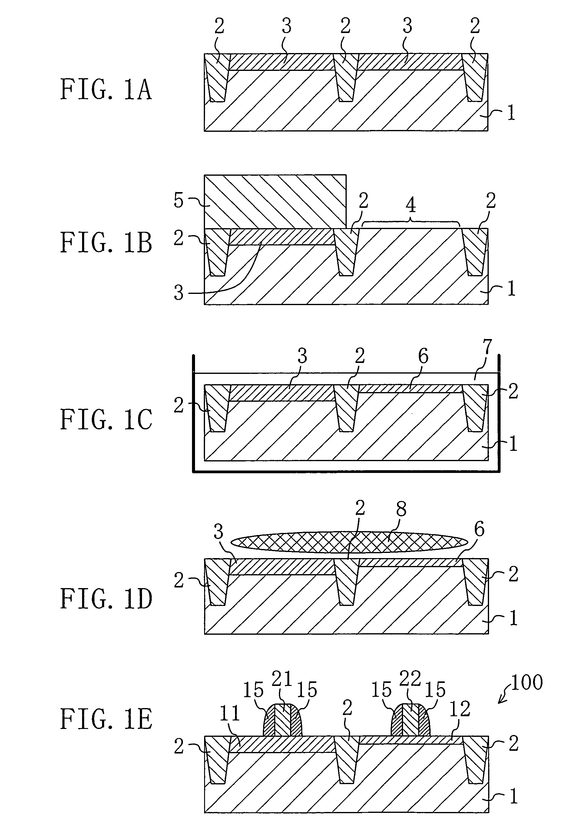
embodiment 1
[0056]EMBODIMENT 1 relates to a semiconductor device including two different gate insulating films having different thicknesses.
[0057]First, a substrate including a silicon layer at least on a surface thereof is prepared. The substrate may be a silicon substrate or an SOI substrate. Moreover, if an epitaxial wafer in which a surface layer of a silicon layer is an epitaxial layer is used, no deficiency is generated in the surface layer. Accordingly, a gate insulating film with excellent film quality can be preferably formed.
[0058]Next, an isolation region is formed in the substrate using STI process.
[0059]Thereafter, a first oxide film for dealing with a relatively high voltage signal such as an input / output signal is formed on the surface of the substrate by thermal oxidation. The thickness of the oxide film is about 7–10 nm. Note that a method for forming a first oxide film is not limited to thermal oxidation but may be plasma oxidation, oxidation using perchloric acid solution or ...
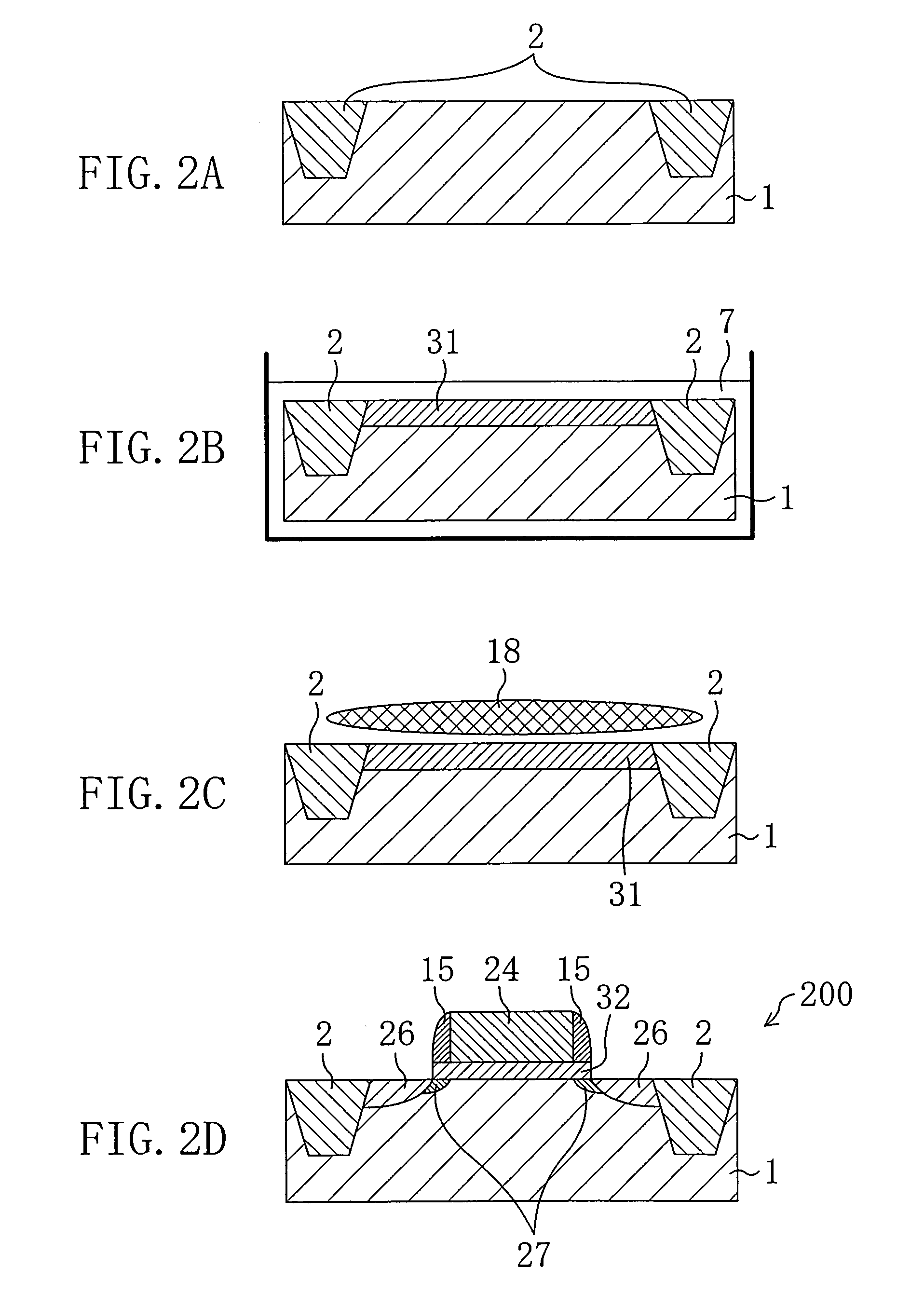
embodiment 2
[0069]EMBODIMENT 2 is different from EMBODIMENT 1 in that three different oxide films having different thicknesses are formed. EMBODIMENT 2 will be described with a focus on this different point of EMBODIMENT 2 from EMBODIMENT 1.
[0070]First and second oxide films are formed in a substrate as in the same manner as in EMBODIMENT 1.
[0071]Next, a photoresist is provided as a mask so as to cover parts of the first and second oxide films which are to be left as first and second gate insulating films, respectively, and then other parts of the first oxide film and / or the second oxide film are removed by etching.
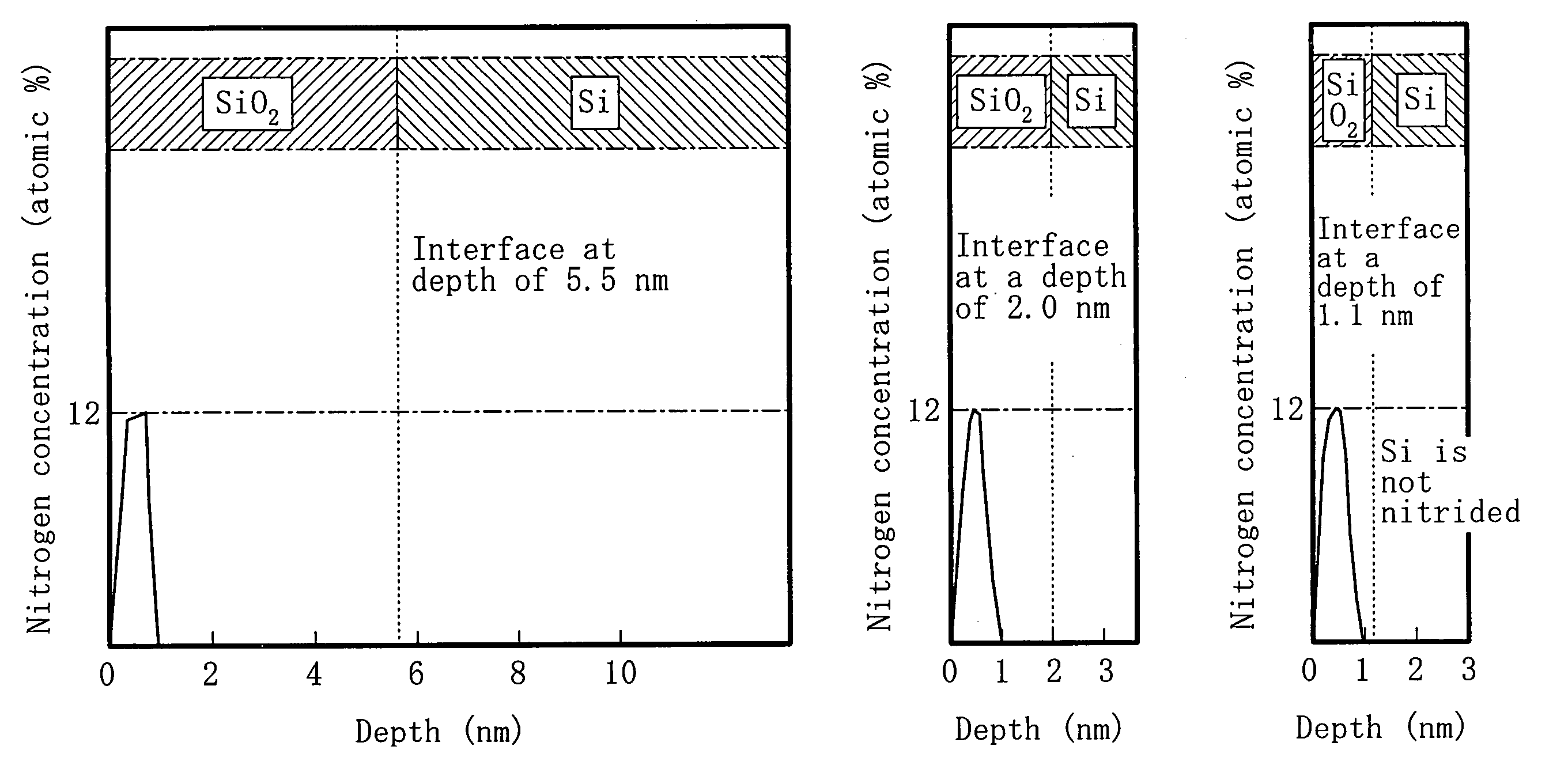
[0072]After the photoresist has been removed, the substrate is immersed in heated nitric acid serving as an oxidizer and then a third oxide film is formed in parts of the substrate from which the first oxide film and / or the second oxide film have been removed by solution oxidation. The thickness of the third oxide film is preferably smaller than that of the second oxide film, i.e., a...
examples
[0075]Hereinafter, examples according to the present invention will be described with reference to the accompanying drawings. In the following drawings, each component having substantially the same function is identified by the same reference numeral for the purpose of simplification.
PUM
 Abstract
Description
Claims
Application Information