CMOS sion gate dielectric performance with double plasma nitridation containing noble gas

a technology of plasma nitridation and gate dielectric performance, which is applied in the direction of basic electric elements, semiconductor/solid-state device manufacturing, electric apparatus, etc., and can solve the problems of increasing the amount of power consumed by the gate, unsatisfactory effects on gate performance and durability, and increasing the leakage of the ga

Inactive Publication Date: 2008-02-07
APPLIED MATERIALS INC
View PDF5 Cites 30 Cited by
  • Summary
  • Abstract
  • Description
  • Claims
  • Application Information

AI Technical Summary

Benefits of technology

[0011]In one embodiment, a method of forming a layer comprising silicon and nitrogen on a substrate comprises introducing a substrate comprising silicon into a chamber and then exposing the substrate in the chamber to a plasma of nitrogen and a noble gas to incorporate nitrogen into an upper surface of the substrate and form a layer comprising silicon and nitrogen on the substrate, wherein the noble gas is selected from the group consisting of argon, neon, krypton, and xenon. The layer comprising silicon and nitrogen is annealed. Annealing the layer may include exposing the layer to gas comprising oxygen gas at a temperature of between about 800° C. and about 1100° C. or exposing the layer to an inert gas at a temperature of between about 800° C. and about 1100° C. The layer is then expose

Problems solved by technology

Attempts have been made to reduce the thickness of SiO2 gate dielectrics below 20 Å. However, it has been found that the use of thin SiO2 gate dielectrics below 20 Å often results in undesirable effects on gate performance and durability.
Also, there is typically an increase in gate leakage, i.e., t

Method used


Image

  • CMOS sion gate dielectric performance with double plasma nitridation containing noble gas
  • CMOS sion gate dielectric performance with double plasma nitridation containing noble gas
  • CMOS sion gate dielectric performance with double plasma nitridation containing noble gas

Examples


Embodiment Construction

[0018]Embodiments of the present invention provide a method of forming a layer comprising silicon and nitrogen. The layer comprising silicon and nitrogen may be a silicon oxynitride (SiON) layer that may be used as a gate dielectric layer. Gate stacks including silicon oxynitride layers according to embodiments of the invention have desirable drive currents in both NMOS and PMOS devices.

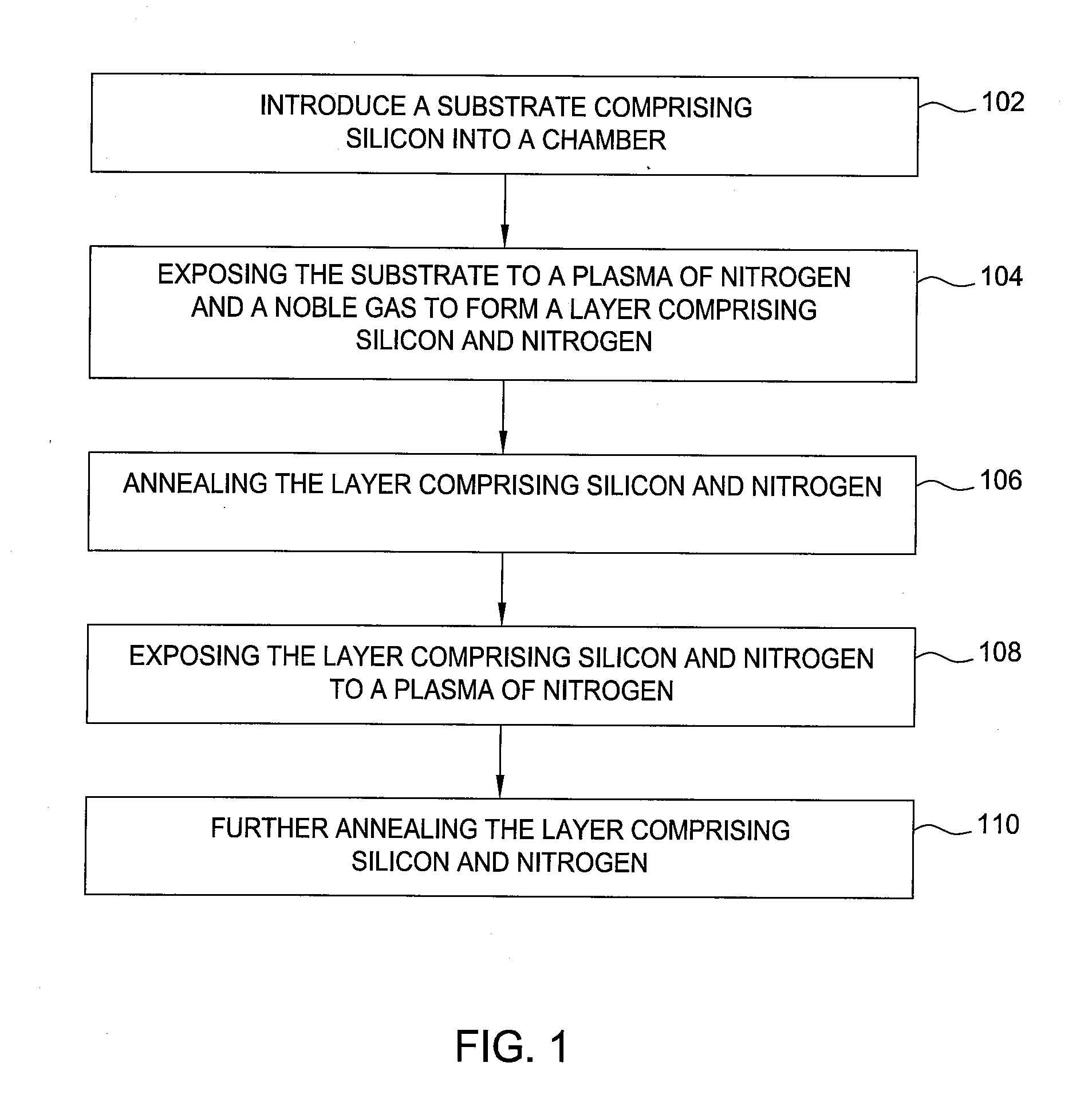
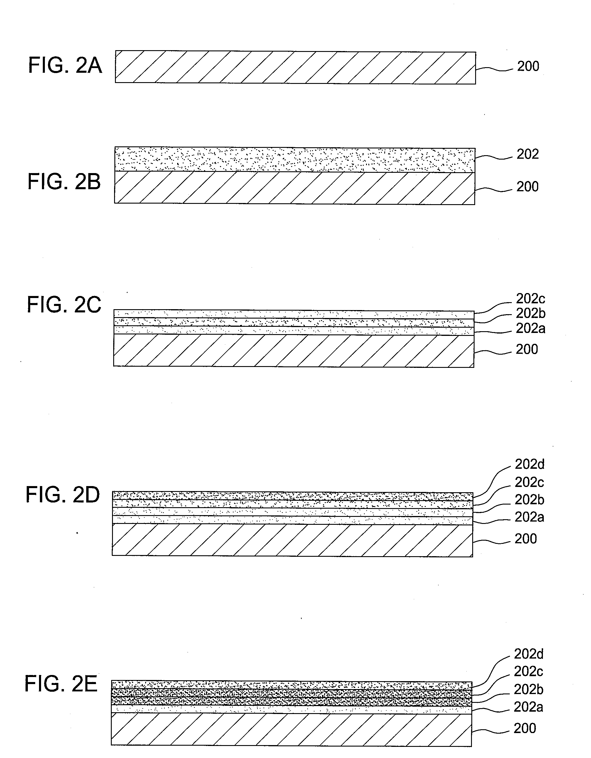
[0019]An embodiment of the invention will be described briefly with respect to the flow chart of FIG. 1 and will be further described below with respect to FIGS. 2A-2E.

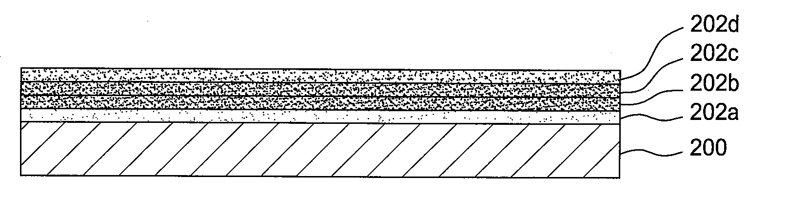
[0020]A substrate comprising silicon is introduced into a chamber at step 102, as shown in FIG. 1. The substrate is exposed to a plasma of nitrogen and a noble gas, i.e., a nitrogen and noble gas-containing-plasma, to form a layer comprising silicon and nitrogen on the substrate, as shown in step 104. The layer comprising silicon and nitrogen is then annealed in step 106. The layer comprising silicon and nitrogen is then exposed to a p...


PUM


Abstract

A method of forming a layer comprising silicon and nitrogen on a substrate is provided. The layer may also include oxygen and be used as a silicon oxynitride gate dielectric layer. In one aspect, forming the layer includes exposing a silicon substrate to a plasma of nitrogen and a noble gas to incorporate nitrogen into an upper surface of the substrate, wherein the noble gas is argon, neon, krypton, or xenon. The layer is annealed and then exposed to a plasma of nitrogen to incorporate more nitrogen into the layer. The layer is then further annealed.

Description

CROSS-REFERENCE TO RELATED APPLICATIONS[0001]This application claims benefit of U.S. provisional patent application Ser. No. 60 / 821,472, filed Aug. 4, 2006, which is herein incorporated by reference.BACKGROUND OF THE INVENTION[0002]1. Field of the Invention[0003]Embodiments of the present invention generally relate to a method of forming a gate dielectric layer. More particularly, embodiments of the invention relate to a method of forming a silicon oxynitride (SiON) gate dielectric layer.[0004]2. Description of the Related Art[0005]Integrated circuits are composed of many, e.g., millions, of devices such as transistors, capacitors, and resistors. Transistors, such as field effect transistors, typically include a source, a drain, and a gate stack. The gate stack typically includes a substrate, such as a silicon substrate, a gate dielectric, such as silicon dioxide, SiO2, on the substrate, and a gate electrode, such as polycrystalline silicon, on the gate dielectric.[0006]As integrate...

Claims


Application Information

Patent Timeline
IPC IPC(8): H01L21/31
CPCH01L21/3144H01L21/823857H01L21/3211H01L21/3185H01L21/02323H01L21/02252H01L21/20H01L21/02337H01L21/02329
Inventor OLSEN, CHRISTOPHER
Owner APPLIED MATERIALS INC
Why Eureka
Try Eureka