Method of forming a capacitor dielectric layer

a dielectric layer and capacitor technology, applied in the field of capacitors, can solve the problems of increasing the cost or process complexity of conventional siosub>2 /sub>, causing the pinhole to become particularly problematic, and undesirably producing very small pinholes in the silicon nitride layer, etc., to achieve the effect of increasing the dielectric constant of the dielectric region

Inactive Publication Date: 2005-04-05
MICRON TECH INC
View PDF119 Cites 29 Cited by
  • Summary
  • Abstract
  • Description
  • Claims
  • Application Information

AI Technical Summary

Benefits of technology

The invention includes capacitors, methods of forming capacitors and methods of forming capacitor dielectric layers. In one implementation, a method of forming a capacitor includes forming first and second capacitor electrodes over a substrate. A capacitor dielectric region is formed intermediate the first and second capacitor electrodes, and includes forming a silicon nitride comprising layer over the first capacitor electrode. A silicon oxi

Problems solved by technology

As integrated circuitry density increases, there is a continuing challenge to maintain sufficiently high storage capacitance despite decreasing capacitor area.
Most of these materials do, however, add increased process complexity or cost over utilization of conventional SiO2 and Si3N4 capacitor dielectric materials.
This can, however, unde

Method used


Image

  • Method of forming a capacitor dielectric layer
  • Method of forming a capacitor dielectric layer
  • Method of forming a capacitor dielectric layer

Examples


Embodiment Construction

This disclosure of the invention is submitted in furtherance of the constitutional purposes of the U.S. Patent Laws “to promote the progress of science and useful arts” (Article 1, Section 8).

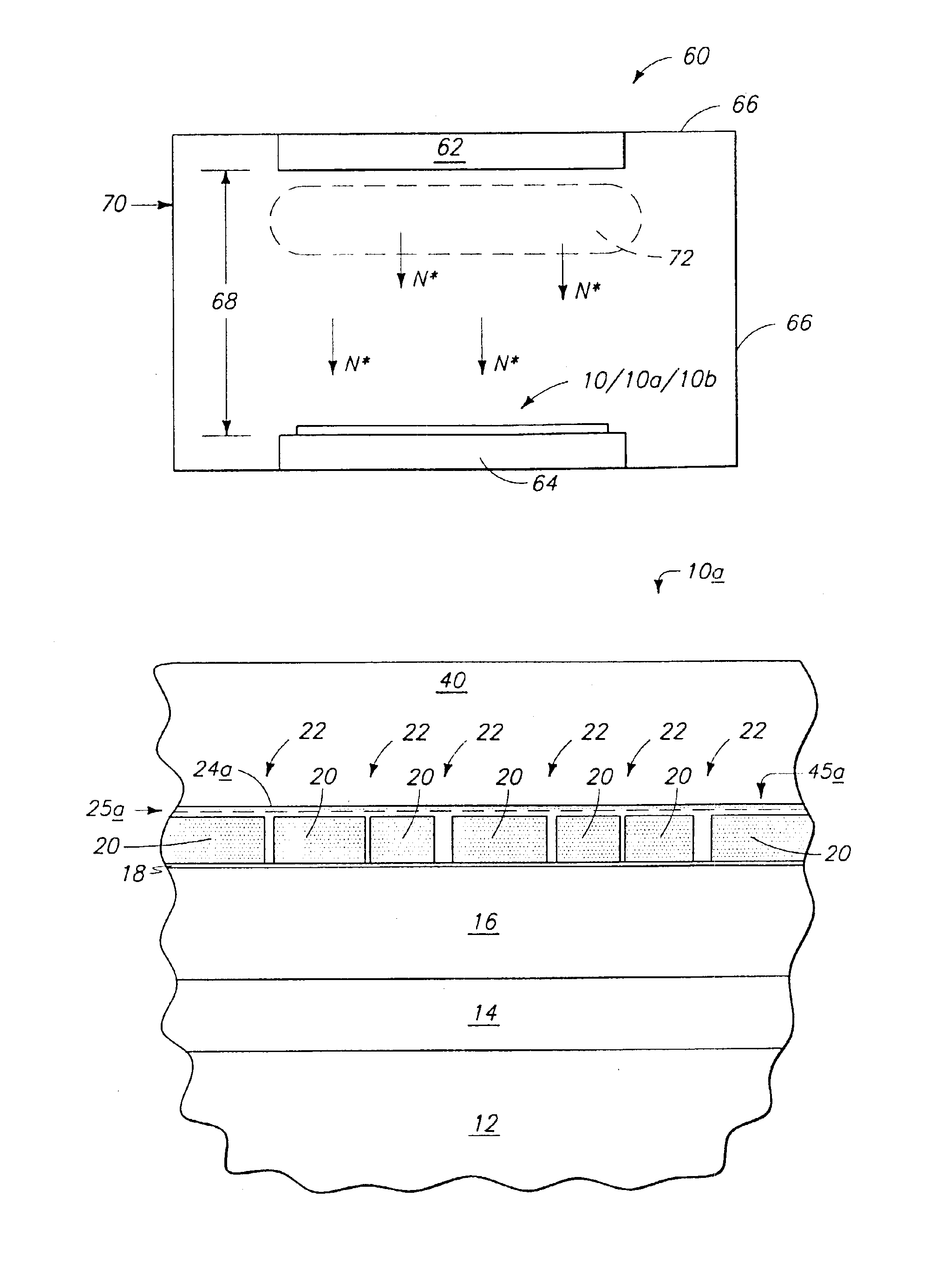
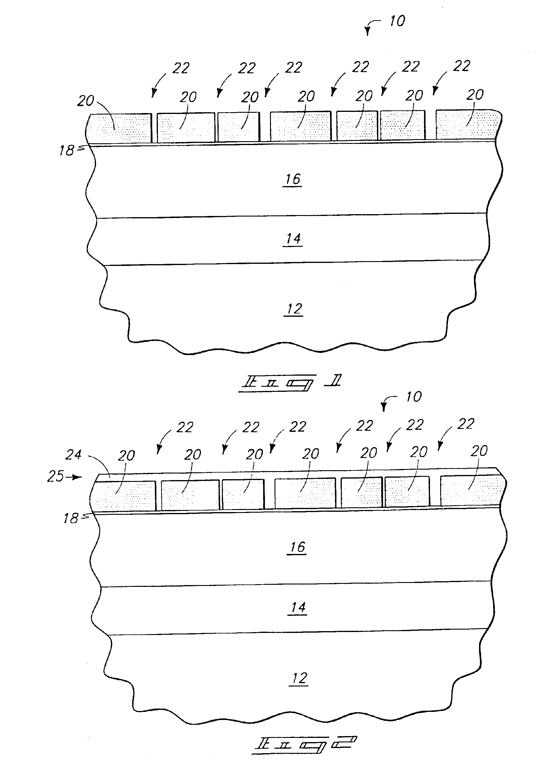
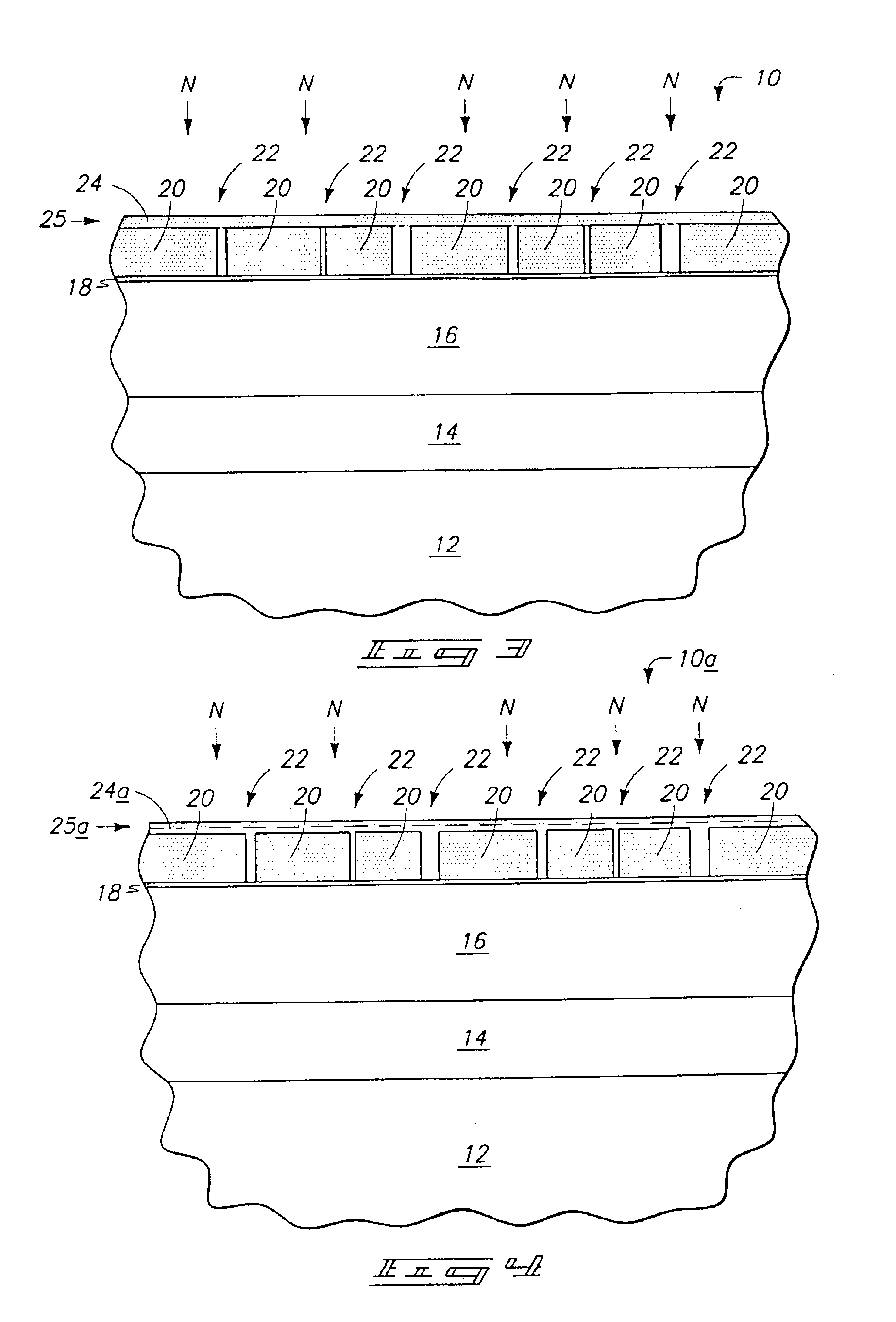
A wafer fragment in process in accordance with a method of forming a capacitor in accordance with an aspect of the invention is indicated generally with reference numeral 10. Such comprises a bulk monocrystalline silicon substrate 12. In the context of this document, the term “semiconductor substrate” or “semiconductive substrate” is defined to mean any construction comprising semiconductive material, including, but not limited to, bulk semiconductive materials such as a semiconductive wafer (either alone or in assemblies comprising other materials thereon), and semiconductive material layers (either alone or in assemblies comprising other materials). The term “substrate” refers to any supporting structure, including, but not limited to, the semiconductive substrates described above. An insulat...


PUM


Abstract

A method of forming a capacitor includes forming first and second capacitor electrodes over a substrate. A capacitor dielectric region is formed intermediate the first and second capacitor electrodes, and includes forming a silicon nitride comprising layer over the first capacitor electrode. A silicon oxide comprising layer is formed over the silicon nitride comprising layer. The silicon oxide comprising layer is exposed to an activated nitrogen species generated from a nitrogen-containing plasma effective to introduce nitrogen into at least an outermost portion of the silicon oxide comprising layer. Silicon nitride is formed therefrom effective to increase a dielectric constant of the dielectric region from what it was prior to said exposing. Capacitors and methods of forming capacitor dielectric layers are also disclosed.

Description

TECHNICAL FIELDThis invention relates capacitors, to methods of forming capacitors and to methods of forming capacitor dielectric layers.BACKGROUND OF THE INVENTIONCapacitors are commonly-used electrical components in semiconductor circuitry, for example in DRAM circuitry. As integrated circuitry density increases, there is a continuing challenge to maintain sufficiently high storage capacitance despite decreasing capacitor area. A typical capacitor is comprised of two conductive electrodes separated by a non-conducting dielectric region. The dielectric region is preferably comprised of one or more materials preferably having a high dielectric constant and low leakage current characteristics. Example materials include silicon oxides, such as SiO2, and Si3N4. Si3N4 is typically preferred due to its higher dielectric constant than SiO2.Numerous capacitor dielectric materials have been and are being developed in an effort to meet the increasing stringent requirements associated with th...

Claims


Application Information

Patent Timeline
IPC IPC(8): H01L21/02H01L21/314
CPCH01L28/40H01L21/3144H01L21/022
Inventor MOORE, JOHN T.DEBOER, SCOTT J.
Owner MICRON TECH INC
Why Eureka
Try Eureka