Layer member forming method

a technology of layer member and forming method, which is applied in the direction of coating, coating, chemical vapor deposition coating, etc., to achieve the effect of easy forming to desired thickness in a short time, no damage, and short tim

Inactive Publication Date: 2006-01-10
SEMICON ENERGY LAB CO LTD
View PDF192 Cites 363 Cited by
  • Summary
  • Abstract
  • Description
  • Claims
  • Application Information

AI Technical Summary

Benefits of technology

[0016]According to such a method of the present invention, since the first layer is deposited by the photo CVD technique on the substrate, even if the substrate surface is uneven, the first layer can be deposited in close contact with the substrate surface and with substantially no damage thereon. Accordingly, the first layer does not substantially contain the material forming the substrate surface, or the substrate surface does not substantially contain the material forming the first layer. Further, the deposition of the first layer is not accompanied by provision of an undesirable interface level between the first layer and the substrate and the application of internal stresses to the first layer and the substrate. In addition, since the second layer is deposited by the plasma CVD technique on the first layer, the second layer can easily be formed to a desired thickness in a short time.
[0017]In accordance with an aspect of the present invention, by forming the first and second layers as insulating, protecting or conductive layers of the same or different types or compositions, the layer member as a insulating, protecting or conductive layer member of desired characteristics can easily be deposited to desired thickness in a short time without inflicting damage on the substrate surface.
[0018]In accordance with another aspect of the present invention, by forming the first and second layers as semiconductive layers of the same type or composition, the layer member as a semiconductor

Problems solved by technology

Further, the deposition of the first layer is not accompanied by provision of an undesirable interface level betwe

Method used


Image

  • Layer member forming method

Examples


embodiment 1

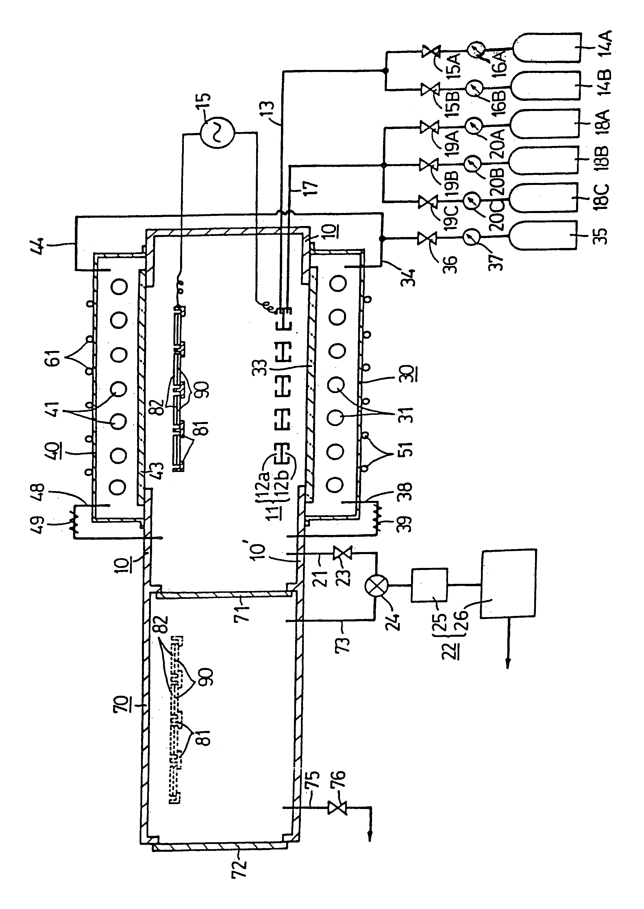
[0039]A description will given of a first embodiment of the present invention for forming the layer member as a insulating layer member on the substrate member 90.

[0040](1) The shutter means 71 between the reaction chamber 10 and the substrate take-in / take-out chamber 70, the shutter means 72 of the chamber 70 a valve 76 between the chamber 70 and the outside, the valves 15A and 15B between the nozzle parts 12a and the gas sources 14A and 14B, the valve 19A, 19B and 19C between the nozzle parts 12b and the gas sources 18A, 18B and 18C and the valve 36 between the chambers 30 and 40 and the gas source 35 are closed.

[0041](2) Next, the valve 23 between the reaction chamber 10 and the vacuum pump system 22 is opened and change-over valve 24 is also opened to the both chambers 10, 70, 30 and 40 to a pressure of 10−7 Torr.

[0042](3) Next, the turbo pump 25 and the rotary pump 26 of the vacuum pump system 22 are activated, evacuating the chambers 10 and 70.

[0043](4) Next, the valve 23 is c...

embodiment 2

[0071]Next, a description will be given of a second embodiment of the present invention for forming a semiconductor layer member as a layer member on a substrate.

[0072]This embodiment forms an amorphous silicon layer as the semiconductor layer member on the substrate 90 by the same steps as those in Embodiment 1 except the following steps.

[0073](12′) In step (12) in Embodiment 1 the heating temperature of the substrate 90 is changed from 350 C to 250 C.

[0074](14′) In step (14) of Embodiment 1 only the disilane (Si2H6) gas is introduced into the chamber 10 and the pressure in the chamber 10 is changed from 3 Torr to 2.5 Torr. A first amorphous silicon layer is deposited as a first semiconductor layer on the substrate 90.

[0075](15′) In step (15) of Embodiment 1, when the first amorphous silicon layer, instead of the first silicon nitride layer, is deposited about 1000 A thick on the substrate member 90, the disilane is discharged or excited into a plasma in place of the gas mixture of...

embodiment 3

[0077]Next, a description will be given of a third embodiment of the present invention which forms an aluminum nitride (AlN) layer member as a insulating layer member on a substrate.

[0078]Embodiment 3 employs a same steps as those in Embodiment 1 except the following steps.

[0079](14′) In step (14) of Embodiment 1 methyl aluminum (Al(CH3)3), instead of the disilane, is introduced from the gas source 14A into the chamber 10, whereby a first aluminum nitride (AlN) layer is deposited as a first insulating layer on the substrate 90. In this case, the deposition rate of the first aluminum nitride layer is 230 A / min.

[0080](15′) In step (15) of Embodiment 1 a second aluminum nitride layer, instead of the second silicon nitride layer, is deposited on the first aluminum nitride layer.

[0081]While in the foregoing the present invention has been described in connection with the cases of forming an insulating layer member having two insulating layers of the same material and a semiconductor layer...


PUM

PropertyMeasurementUnit
aaaaaaaaaa

Abstract

A vapor reaction method including the steps of providing a pair of first and second electrodes within a reaction chamber where the pair of electrodes are arranged substantially parallel with each other. The method further includes the steps of placing a substrate in the reaction chamber where the substrate is held by said first electrode so that a first surface of the substrate faces toward the second electrode. A first film forming gas is introduced into the reaction chamber through the second electrode. The first film forming gas is excited to form a first insulating film by vapor deposition. The first insulating film may be silicon nitride. The method may also include the step of introducing a second film forming gas into the reaction chamber through the second electrode to ultimately form a second film. After removing the substrate from the reaction chamber, a cleaning gas may then be introduced through the second electrode to remove unnecessary layers from the inside of the reaction chamber.

Description

[0001]This application is a DIV of Ser. No. 08 / 659,636 Jun. 6, 1996 ABN which is a DIV of Ser. No. 08 / 351,140 Nov. 30, 1994 U.S. Pat. No. 5,650,013 which is a CON of Ser. No. 08 / 064,212 May 12, 1993 ABN which is a DIV of Ser. No. 07 / 842,758 Feb. 28, 1992 ABN which is a CON of Ser. No. 07 / 595,762 Oct. 3, 1990 ABN which is a CON of Ser. No. 07 / 312,420 Feb. 21, 1989 ABN which is a CON of Ser. No. 07 / 092,130 Sep. 2, 1987 ABN which is a DIV of Ser. No. 06 / 801,768 Nov. 26, 1985 ABN.BACKGROUND OF THE INVENTION[0002]1. Field of the Invention[0003]The present invention relates to a layer member forming method which is suitable for use in the fabrication of various electronic devices of the type having an insulating, protecting, conductive, semiconductor or like layer member formed on a substrate member.[0004]2. Description of the Prior Art[0005]Heretofore there has proposed a method for forming such a layer member on a substrate member through use of a photo CVD or plasma CVD process.[0006]A...

Claims


Application Information

Patent Timeline
IPC IPC(8): H01L21/31H05H1/00C23C16/44C23C16/48C23C16/50C23C16/54H01L21/205H01L21/263H01L21/302
CPCC23C16/4405C23C16/54C23C16/482H01L21/0245H01L21/02532H01L21/0262H01L21/02488
Inventor YAMAZAKI, SHUNPEI
Owner SEMICON ENERGY LAB CO LTD
Why Eureka
Try Eureka