Method of forming silicon-containing films

a technology of silicon-containing films and silicon-containing materials, which is applied in the direction of semiconductor/solid-state device manufacturing, basic electric elements, electric apparatus, etc., can solve the problems that silicon-containing films deposited at temperatures below 400° c. exhibit poor film qualities

Inactive Publication Date: 2009-03-19
LAIR LIQUIDE SA POUR LETUDE & LEXPLOITATION DES PROCEDES GEORGES CLAUDE
View PDF9 Cites 364 Cited by
  • Summary
  • Abstract
  • Description
  • Claims
  • Application Information

AI Technical Summary

Benefits of technology

[0015]d) reacting the substrate, silicon-containing compound, and co-reactant in the gaseous form at a te

Problems solved by technology

Attempts have been made to reduce the temperature deposition of such SiN films, to reach a temperature which is not

Method used


Image

  • Method of forming silicon-containing films
  • Method of forming silicon-containing films
  • Method of forming silicon-containing films

Examples


example 1a

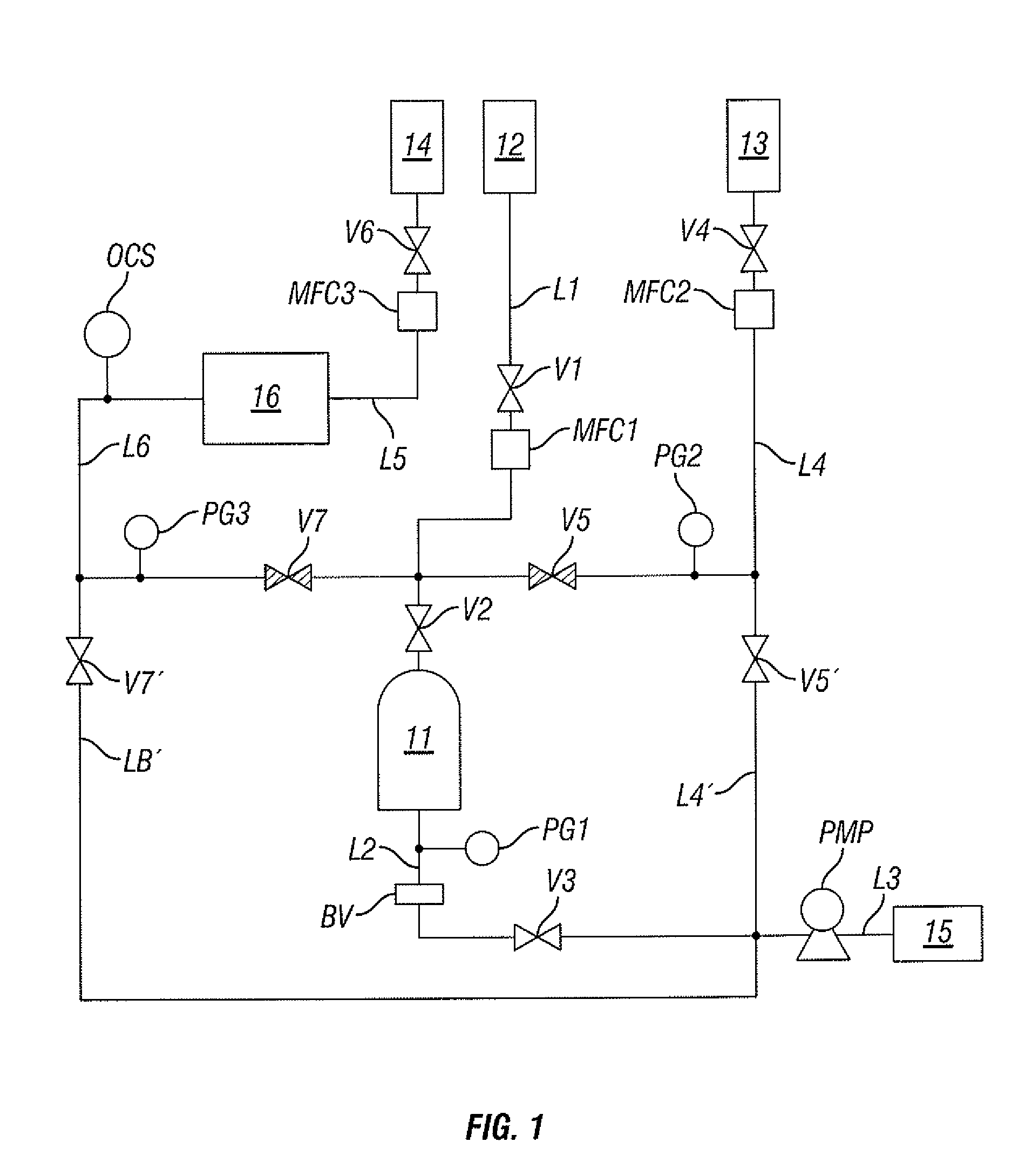
[0086]A silicon wafer was positioned on the susceptor in the reaction chamber 11 and the wafer was heated to 500° C. A silicon oxide film was formed by repeating a cycle comprising the steps of 1) nitrogen gas purge, 2) silicon-containing compound gas pulse, 3) nitrogen gas purge, and 4) ozone+oxygen mixed gas pulse as described herein previously using the following conditions:

[0087]1) Nitrogen gas purge[0088]pressure within the reaction chamber: 3 torr[0089]nitrogen gas feed flow rate: 130 sccm[0090]nitrogen gas purge time: 6 seconds

[0091]2) Silicon-containing compound gas pulse[0092]pressure within the reaction chamber: 3 torr[0093]Si compound gas: bis(diethylamino)silane (BDEAS) gas[0094]BPDEAS gas feed flow rate: 2 sccm[0095]BDEAS pulse time: 1 second

[0096]3) Nitrogen gas purge[0097]pressure within the reaction chamber: 3 torr[0098]nitrogen gas feed flow rate: 130 sccm[0099]nitrogen gas purge time: 6 seconds

[0100]4) Ozone+oxygen mixed gas pulse[0101]pressure within the reaction ...

example 1b

[0104]A silicon wafer was positioned on the susceptor in the reaction chamber 11 and the wafer was heated to 550° C. A silicon nitride film was formed by repeating a cycle comprising the steps of 1) nitrogen gas purge, 2) silicon-containing compound gas pulse, 3) nitrogen gas purge, and 4) hydrazine+ammonia mixed gas pulse as described herein previously using the following conditions:

[0105]1) Nitrogen gas purge[0106]pressure within the reaction chamber: 3 torr[0107]nitrogen gas feed flow rate: 130 sccm[0108]nitrogen gas purge time: 6 seconds

[0109]2) silicon-containing compound gas pulse[0110]pressure within the reaction chamber: 3 torr silicon-containing compound gas: bis(diethylamino)silane (BDEAS) gas[0111]BDEAS gas feed flow rate: 2 sccm[0112]BDEAS pulse time: 1 second

[0113]3) Nitrogen gas purge[0114]pressure within the reaction chamber: 3 torr[0115]nitrogen gas feed flow rate: 130 sccm[0116]nitrogen gas purge time: 6 seconds

[0117]4) Hydrazine+ammonia mixed gas pulse[0118]pressur...

example 1c

[0121]A silicon wafer was positioned on the susceptor in the reaction chamber 11 and the wafer was heated to 500° C. A silicon oxide film was formed by repeating a cycle comprising the steps of 1) nitrogen gas purge, 2) silicon-containing compound gas pulse, 3) nitrogen gas purge, and 4) oxygen pulse while switching on a plasma as described herein previously using the following conditions:

[0122]1) Nitrogen gas purge[0123]pressure within the reaction chamber: 3 torr[0124]nitrogen gas feed flow rate: 130 seem[0125]nitrogen gas purge time: 6 seconds

[0126]2) silicon-containing compound gas pulse[0127]pressure within the reaction chamber: 3 torr[0128]Si compound gas: bis(diethylamino)silane (BDEAS) gas[0129]BDEAS gas feed flow rate: 2 sccm[0130]BDEAS pulse time: 1 second

[0131]3) Nitrogen gas purge[0132]pressure within the reaction chamber: 3 torr[0133]nitrogen gas feed flow rate: 130 sccm[0134]nitrogen gas purge time: 6 seconds

[0135]4) Oxygen pulse[0136]pressure within the reaction chamb...


PUM


Abstract

A method of forming a silicon-containing film comprising providing a substrate in a reaction chamber, injecting into the reaction chamber at least one silicon-containing compound; injecting into the reaction chamber at least one co-reactant in the gaseous form; and reacting the substrate, silicon-containing compound, and co-reactant in the gaseous form at a temperature equal to or less than 550° C. to obtain a silicon-containing film deposited onto the substrate. A method of preparing a silicon nitride film comprising introducing a silicon wafer to a reaction chamber; introducing a silicon-containing compound to the reaction chamber; purging the reaction chamber with an inert gas; and introducing a nitrogen-containing co-reactant in gaseous form to the reaction chamber under conditions suitable for the formation of a monomolecular layer of a silicon nitride film on the silicon wafer.

Description

CROSS-REFERENCE TO RELATED APPLICATIONS[0001]The present application claims the benefit of U.S. Provisional Patent Application No. 60 / 973,210 filed Sep. 18, 2007, the disclosure of which is hereby incorporated herein by reference.FIELD OF INVENTION[0002]This invention relates generally to the field of semiconductor fabrication, and more specifically to methods of forming silicon-containing films. Still more particularly, the invention relates to methods of forming silicon-containing films using a silicon precursor and a co-reactant in the gaseous form.BACKGROUND OF INVENTION[0003]In the front end manufacture of Complementary Metal-Oxide-Semiconductor (CMOS) devices, a passivation film such as silicon nitride (SiN) is formed on the gate electrode of each Metal-Oxide-Semiconductor (MOS) transistor. This SiN film is deposited on the top and side surfaces of the gate electrodes (such as polycrystalline silicon or metallic layers) in order to increase the breakdown voltage of each transi...

Claims


Application Information

Patent Timeline
IPC IPC(8): H01L21/31
CPCH01L21/02164H01L21/0217H01L21/02222H01L21/3185H01L21/0228H01L21/3141H01L21/31612H01L21/02274H01L21/324
Inventor DUSSARRAT, CHRISTIAN
Owner LAIR LIQUIDE SA POUR LETUDE & LEXPLOITATION DES PROCEDES GEORGES CLAUDE
Why Eureka
Try Eureka