Method for forming contact plug in semiconductor device

a technology of contact plug and semiconductor device, which is applied in the direction of semiconductor devices, electrical equipment, basic electric elements, etc., can solve the problems of poor uniformity and step coverage, inability to remove completely the oxide formed at the interface of the contact plug, and inability to perform in-situ cleaning processes. , to achieve the effect of preventing a decrease of contact resistance and deteriorating contact resistance uniformity

Inactive Publication Date: 2005-01-18
CONVERSANT INTPROP MANAGEMENT INC
View PDF7 Cites 77 Cited by
  • Summary
  • Abstract
  • Description
  • Claims
  • Application Information

AI Technical Summary

Benefits of technology

It is, therefore, an object of the present invention to provide a method for forming a contact plug in a semiconductor device capable of preventing a de

Problems solved by technology

For this reason, it is impossible to remove completely the oxide formed at the interface of the contact plug.
In case of forming the contact plug by depositing a silicon thin film through the tube-type deposition equipment, it is possible for the silicon thin film to obtain a good step coverage property but impossible to perform the in-situ cleaning process.
Hence, the silicon thin film is inevitably deposited after performing the ex-situ cleaning process.
However, compared to use of the tube-type depos

Method used


Image

  • Method for forming contact plug in semiconductor device
  • Method for forming contact plug in semiconductor device
  • Method for forming contact plug in semiconductor device

Examples


Embodiment Construction

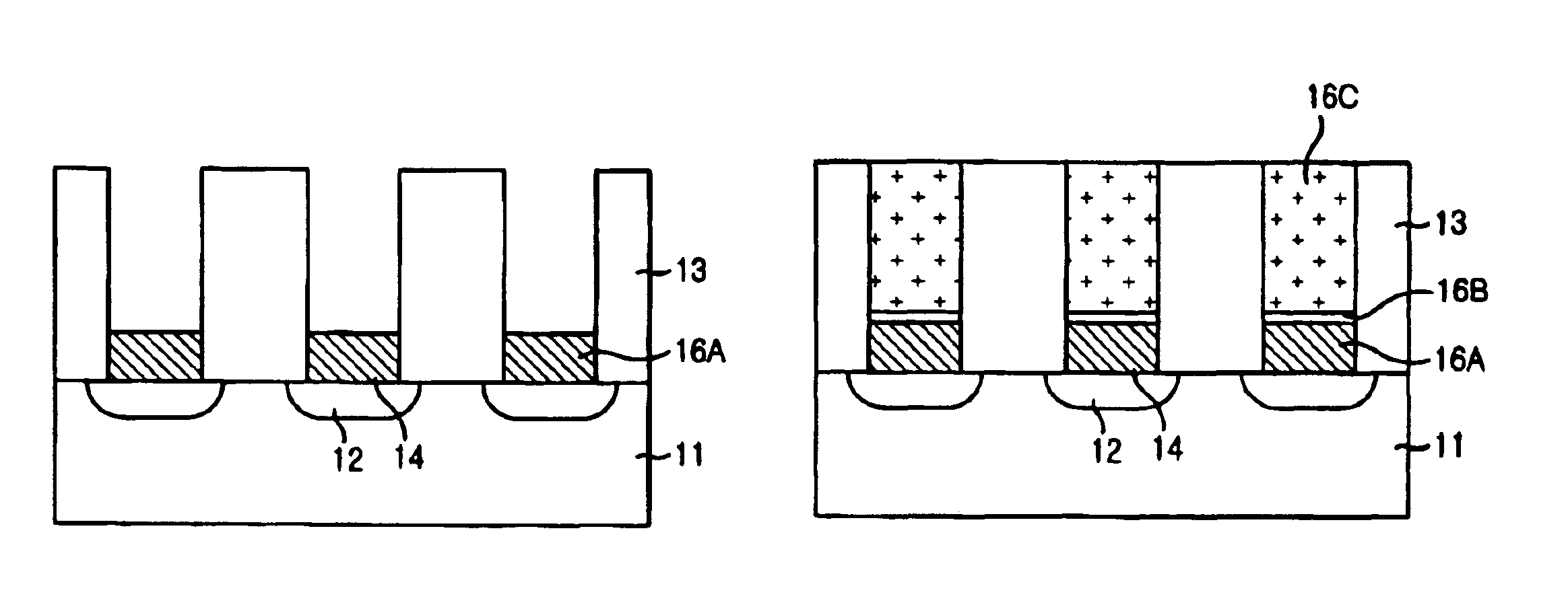
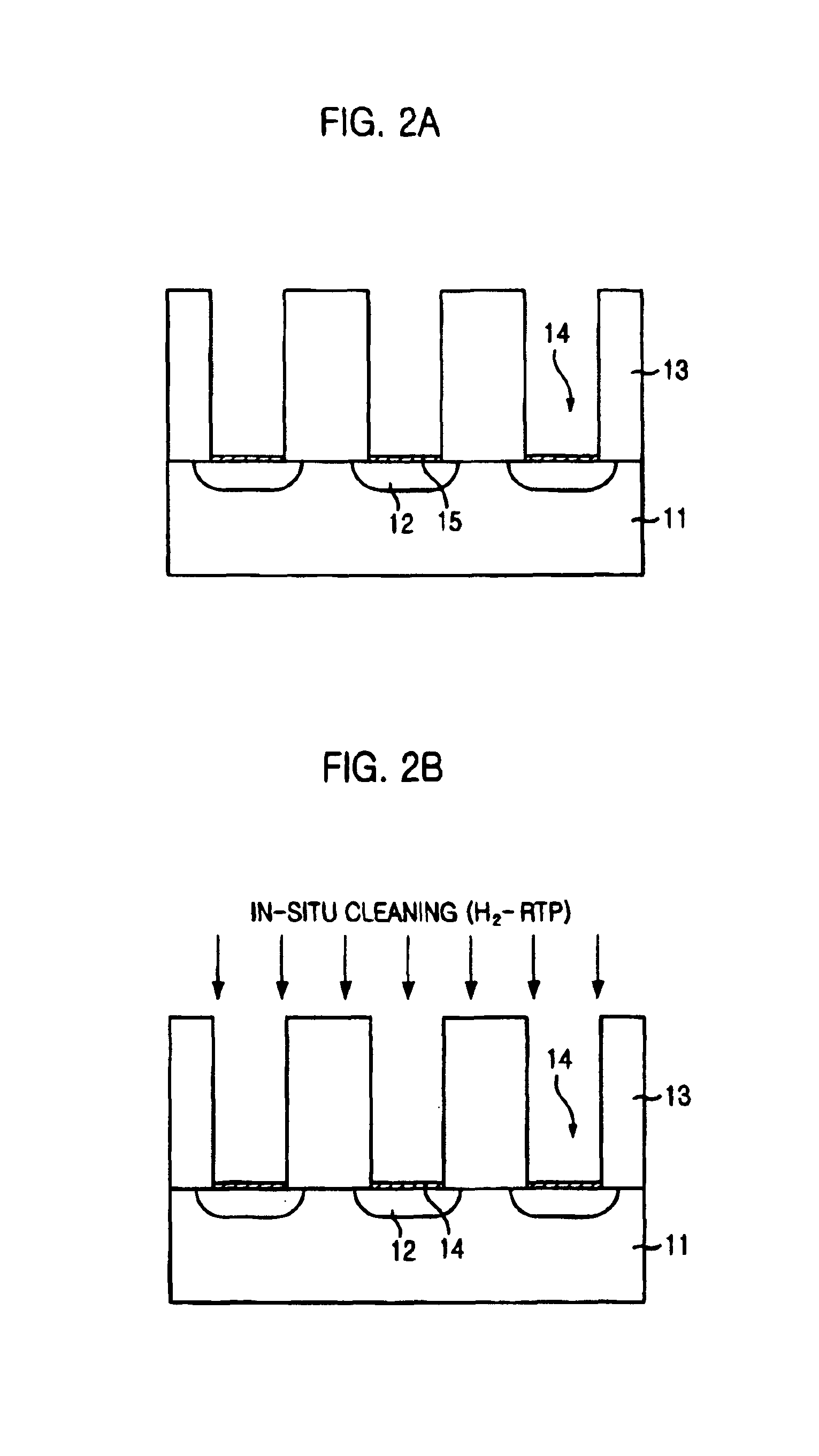
FIGS. 2A to 2E are cross-sectional views illustrating a method for forming a contact plug with a double polysilicon (DPS) thin film in a semiconductor device in accordance with a preferred embodiment of the present invention.

Referring to FIG. 2A, an inter-layer insulating layer 13 is formed on a substrate 11 providing various elements including a junction area 12. Then, a predetermined portion of the inter-layer insulating layer 13 is etched to form a contact hole 14 that exposes the junction area 12 of the substrate 11.

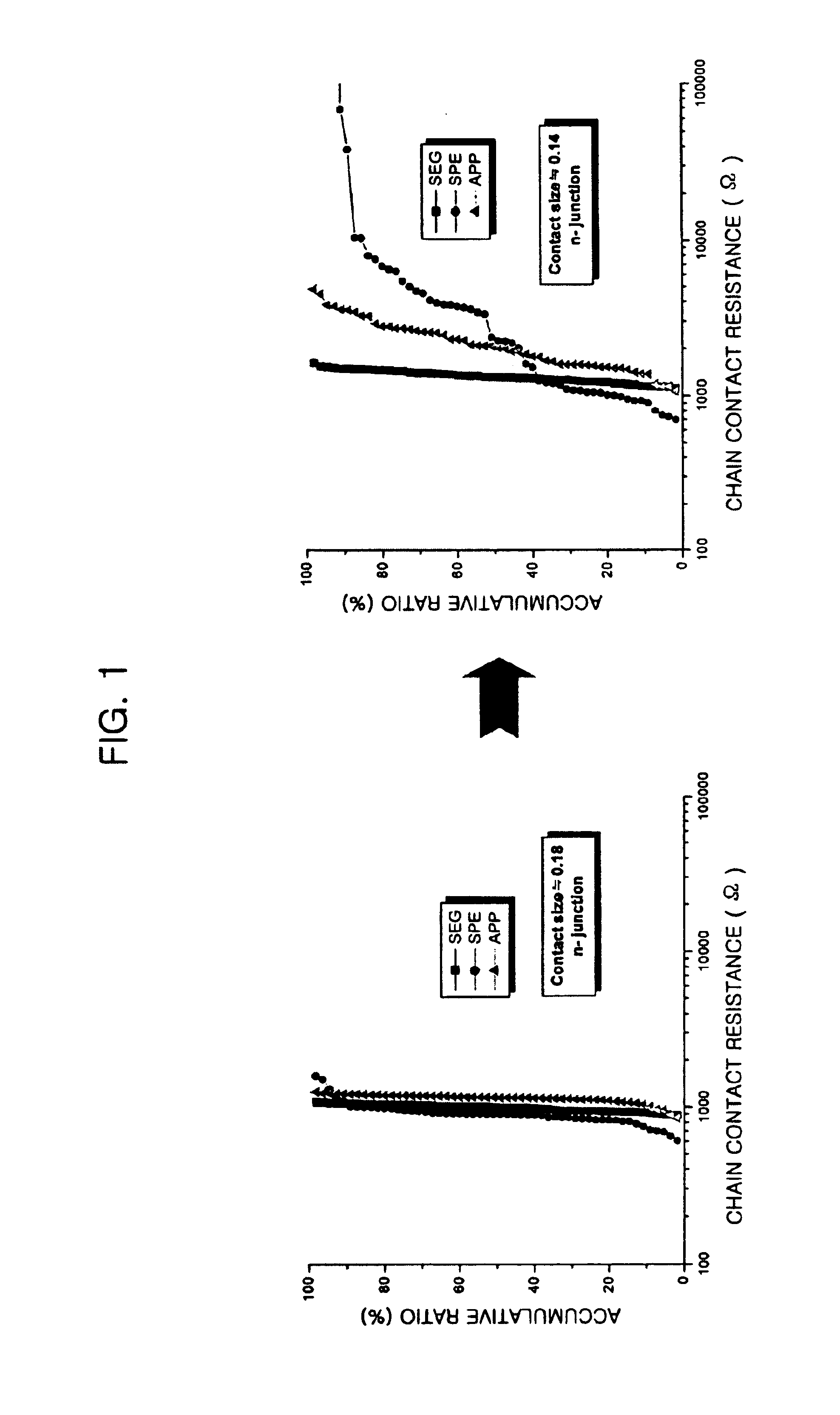
At this time, a native oxide layer 15 is formed on a surface of the junction area 12 exposed through the formation of the contact hole 14. Also, while forming the contact hole 14, there by-produced remnants from the etching and a damaged layer through the etching at the junction area 12. The remnants and the damaged layer degrade a characteristic of leakage currents of a semiconductor device. Also, the native oxide layer 15 increases contact resistance, and thus, bec...


PUM


Abstract

The present invention provides a method for forming a contact plug in a semiconductor device capable of preventing an increase of contact resistance even if the contact size becomes smaller and degradation of a step coverage property and of suppressing a decrease of uniformity in the contact resistance. The inventive method includes the steps of: a method for forming a contact plug in a semiconductor device, comprising the steps of: forming a contact hole by etching an insulating layer on a substrate; forming a first silicon film with a first doping concentration on the substrate in the contact hole so that the contact hole is partially filled; flushing a doping gas on a surface of the first silicon film; and forming a second silicon film having a second doping concentration higher than the first doping concentration on the first silicon film until filling the contact hole.

Description

FIELD OF THE INVENTIONThe present invention relates to a method for fabricating a semiconductor device; and, more particularly, to a method for forming a contact plug with a double polysilicon (DPS) thin film in a semiconductor device.DESCRIPTION OF RELATED ARTSRecently, the size of a contact plug decreases as a level of integration of a semiconductor device progressively advances. Due to this decreased size of the contact plug, contact resistance of a typically used silicon plug conversely increases. Especially, an oxide formed at an interface of the contact plug is one of causes for increasing the contact resistance of the silicon plug with multi-crystals. Hence, a cleaning process is applied to remove the oxide in order to reduce the contact resistance of the silicon plug with multi-crystals.However, in case of removing a layer constructed with the oxide by cleaning a semiconductive substrate through an ex-situ cleaning process, a native oxide layer is formed while the semiconduc...

Claims


Application Information

Patent Timeline
IPC IPC(8): H01L21/02H01L21/285H01L21/70H01L21/768H01L21/311H01L21/306H01L21/28
CPCH01L21/02063H01L21/28525H01L21/76879H01L21/31116H01L21/76814H01L21/28562H01L21/02043H01L21/28
Inventor CHEONG, WOO-SEOCK
Owner CONVERSANT INTPROP MANAGEMENT INC
Why Eureka
Try Eureka