

Method of forming a TFT by adding a metal to a silicon film promoting crystallization, forming a mask, forming another silicon layer with group XV elements, and gettering the metal through opening in the mask
a technology of silicon film and metal, applied in the field of forming a tft, can solve the problems of inability to cope with large-area films, and inability to use a glass substra
- Summary
- Abstract
- Description
- Claims
- Application Information
AI Technical Summary
Problems solved by technology
Method used
Image

Examples
example 2
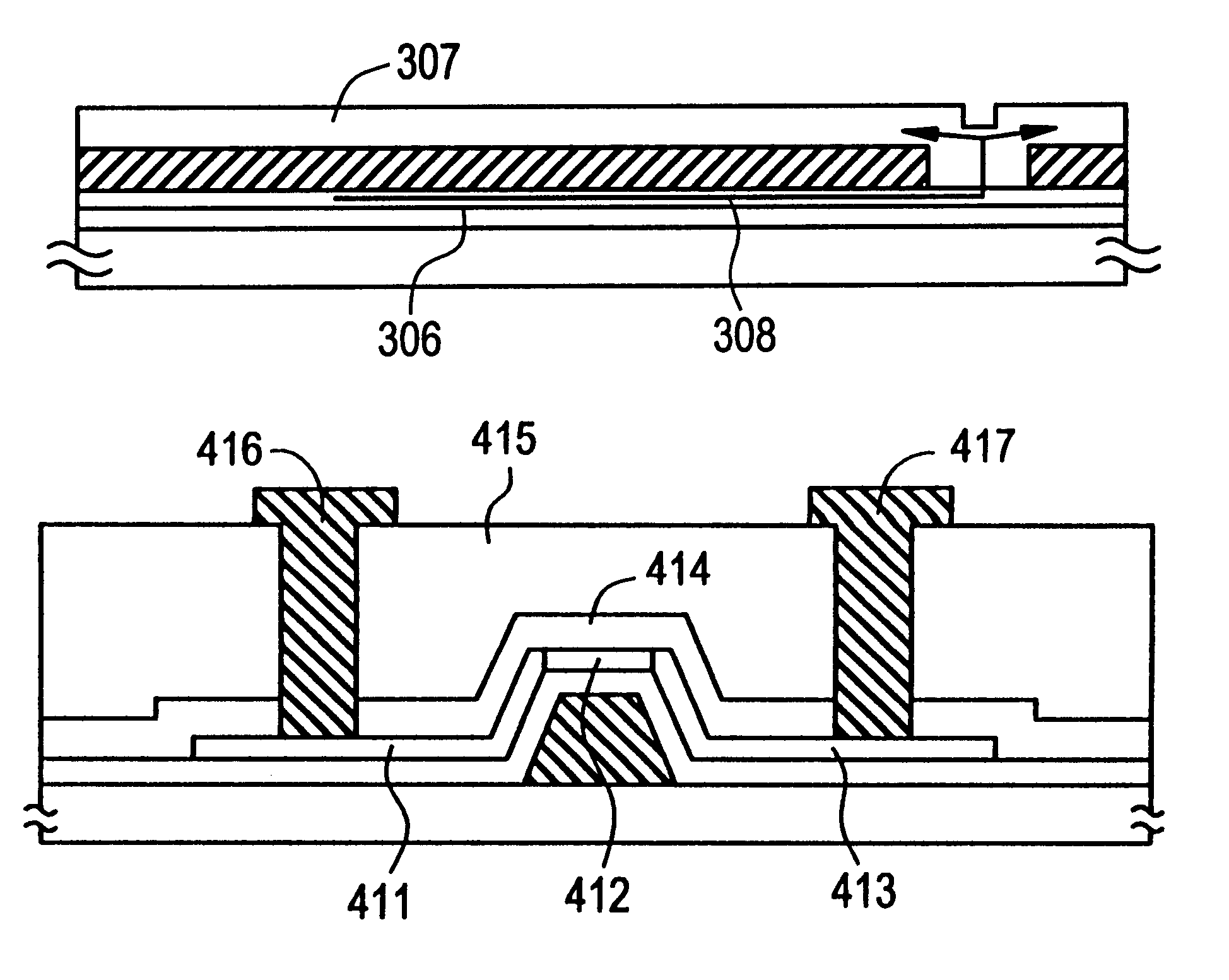
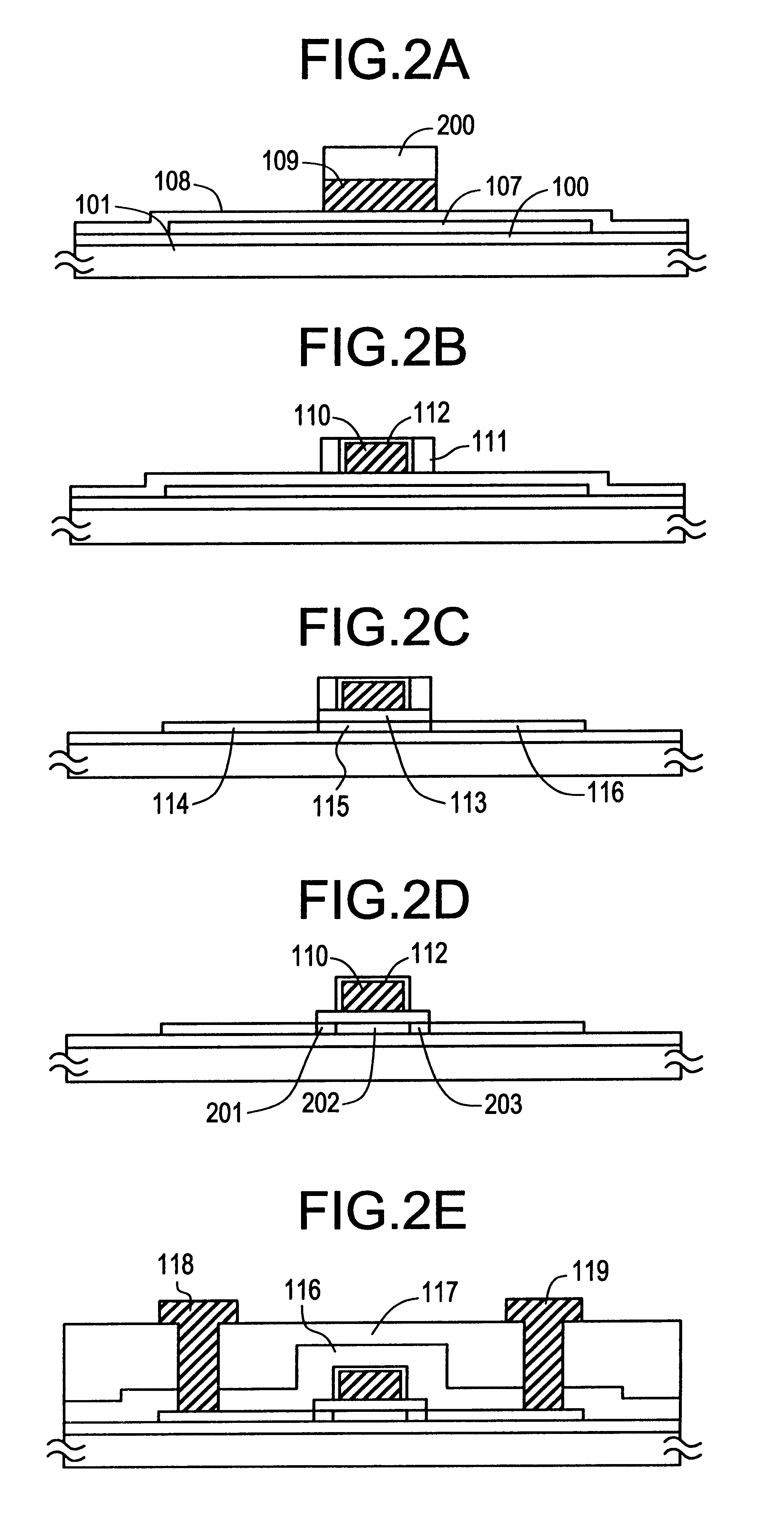
The process sequence of the present example is similar to the process sequence of Example 1 except that a P-channel TFT is manufactured. For this purpose, boron is introduced instead of phosphorus in the steps shown in FIGS. 2(C) and 2(D).
example 3
The process sequence of the present example is similar to the process sequence of Example 1 except that the gate electrode is made of a material other than aluminum. In this example, the gate electrode is made of tungsten silicide.
The gate electrode may be made of various silicides and various metals in addition to the tungsten silicide described above. Furthermore, a silicon material to which conductivity is imparted can be used as the material of the gate electrode. Moreover, the gate electrode may consist of a laminated structure of various conductive materials.
Generally, where aluminum is used, the electrode has the advantage that it exhibits a low resistance. However, the process temperature is limited. On the other hand, where other materials are used, higher resistances are obtained than where aluminum is used. However, higher heat-resistance is obtained. In addition, the process temperature can be elevated.
example 4
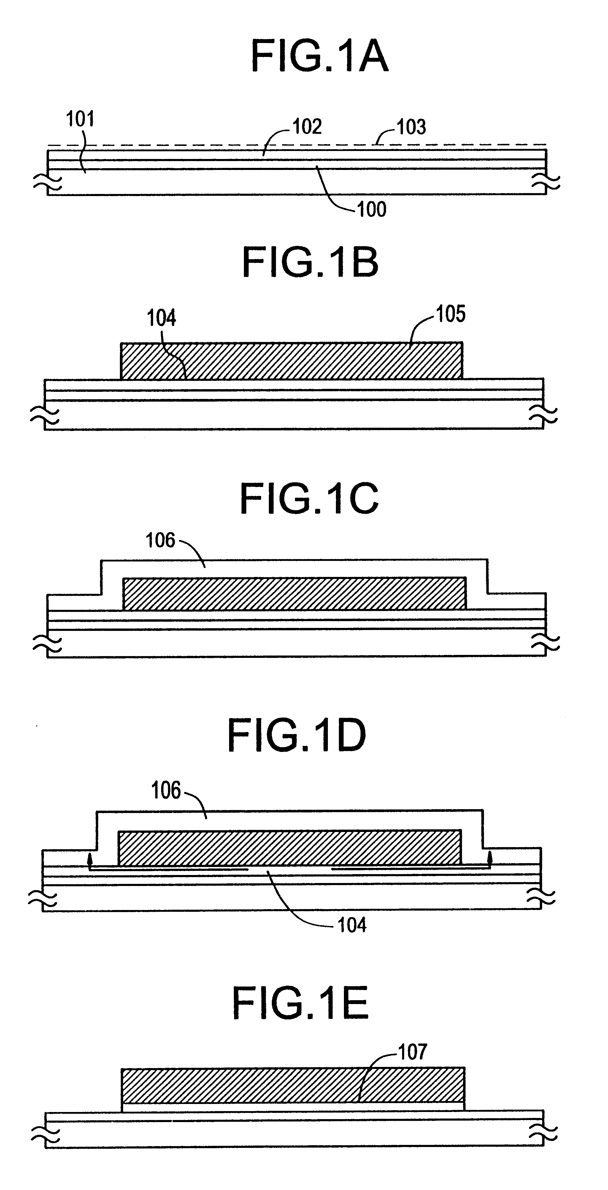
The process sequence of this example is similar to the process sequence of Example 1 except that a process step for removing a trace amount of nickel remaining in the channel region is added to the nickel-gettering step shown in FIG. 1(D).
Execution of the nickel-gettering step shown in FIG. 1(D) lowers the nickel concentration in the region 107 shown in FIG. 1(E) to an unmeasurable level. More specifically, the nickel concentration measured immediately after the crystallization by SIMS (secondary ion mass spectroscopy) is approximately 1.times.10.sup.18 atoms / cm.sup.3 to 5.times.10.sup.19 atoms / cm.sup.3. This can be reduced to below 10.sup.17 atoms / cm.sup.3 by performing the step shown in FIG. 1(D). That is, the concentration of the nickel remaining in the region 107 shown in FIG. 1(E) can be reduced to below 10.sup.17 atoms / cm.sup.3. Accordingly, the concentration of nickel in the TFT manufactured by performing the process sequence of Example 1 can be lowered to below 10.sup.17 ato...
PUM
| Property | Measurement | Unit |
|---|---|---|
| temperature | aaaaa | aaaaa |
| temperature | aaaaa | aaaaa |
| thickness | aaaaa | aaaaa |
Abstract
Description
Claims
Application Information