Low cost flowable dielectric films

a flowable dielectric film, low cost technology, applied in the direction of coatings, metallic material coating processes, chemical vapor deposition coatings, etc., can solve the problems of dielectric material, dielectric material, and structural features of the device having decreased spatial dimensions,

Active Publication Date: 2014-03-13
APPLIED MATERIALS INC
View PDF12 Cites 78 Cited by
  • Summary
  • Abstract
  • Description
  • Claims
  • Application Information

AI Technical Summary

Benefits of technology

[0007]A method of forming a dielectric layer is described. The method deposits a silicon-containing film by chemical vapor deposition using a local plasma. The silicon-containing film is flowable during deposition at low substrate temperature. A silicon precursor (e.g. a silylamine, higher order silane or halogenated silane) is delivered to the substrate processing region and excited in a local plasma. A second plasma vapor or gas is combined with the silicon precursor in the substrate proc...

Problems solved by technology

The decreasing feature sizes result in structural features on the device having decreased spatial dimensions.
The widths of gaps and trenches on the device have narrowed to a point where the aspect ratio of gap depth to its width becomes high enough to make it challenging to fill the gap with dielectric material.
The depositing dielectric material is prone to clog at the top before the gap completely fills, producing a void or seam in the middle of the gap.
However, once these highly flowable material...

Method used


Image

  • Low cost flowable dielectric films
  • Low cost flowable dielectric films
  • Low cost flowable dielectric films

Examples


Embodiment Construction

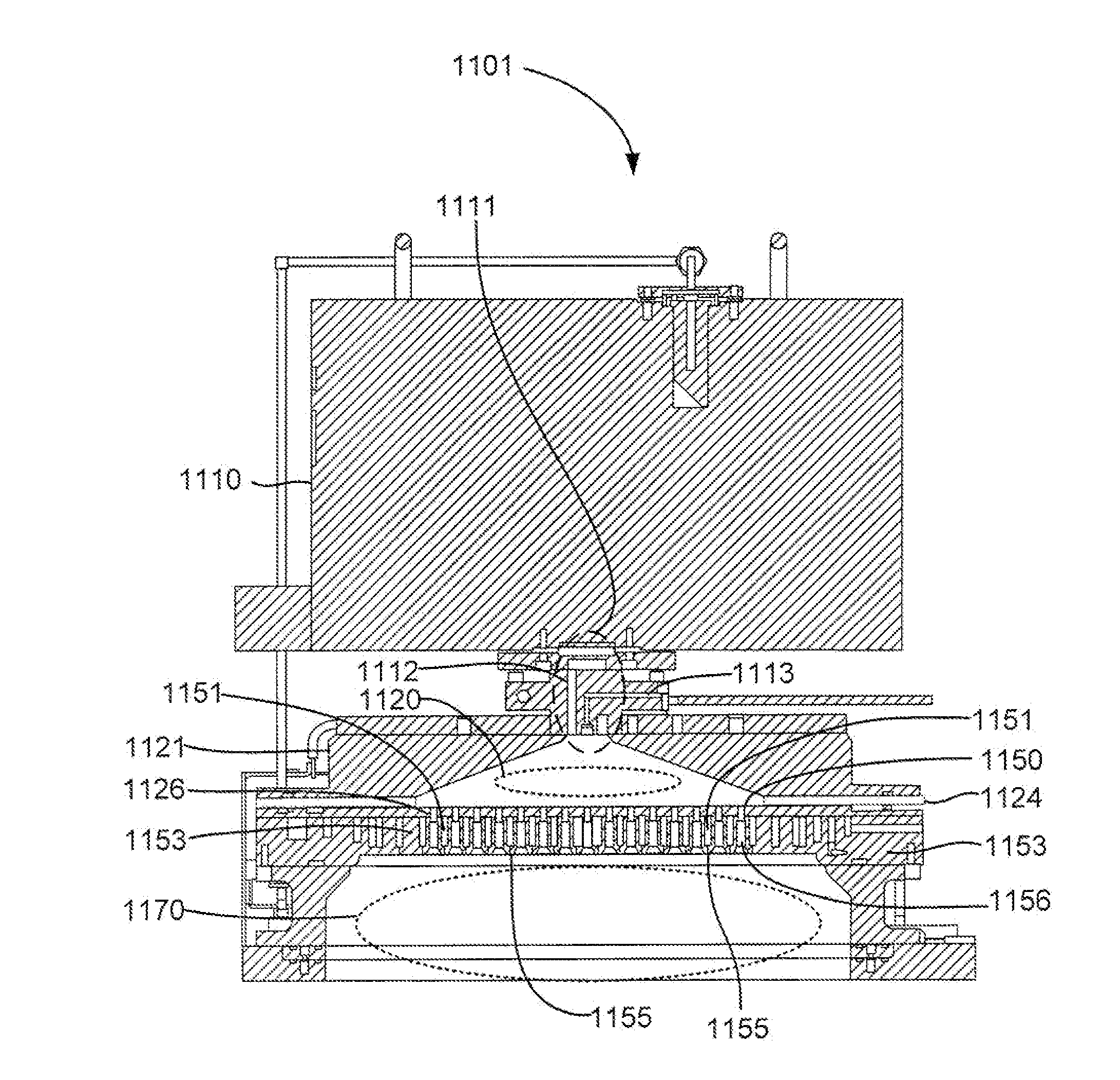
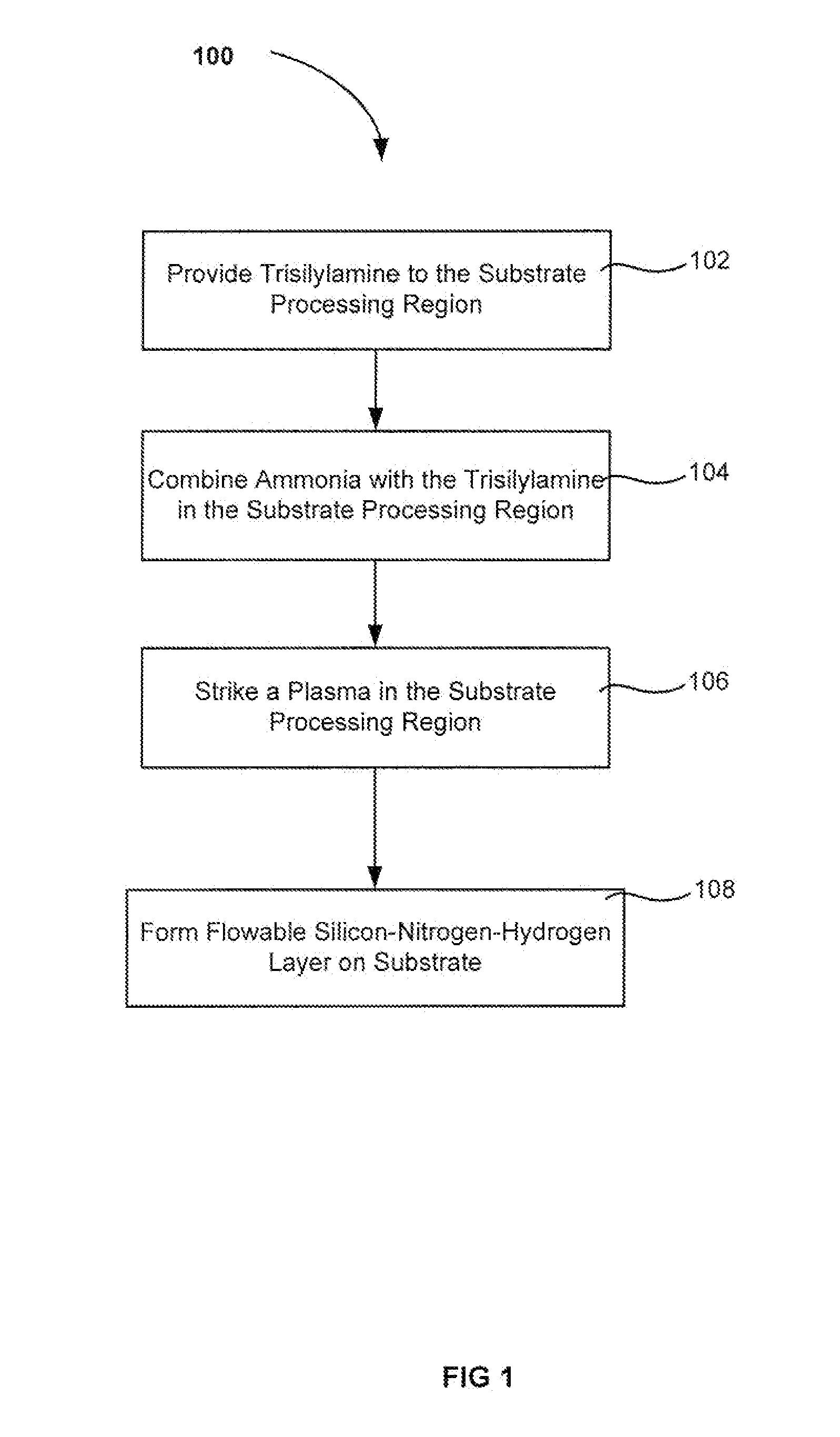
[0015]A method of forming a dielectric layer is described. The method deposits a silicon-containing film by chemical vapor deposition using a local plasma. The silicon-containing film is flowable during deposition at low substrate temperature. A silicon precursor (e.g. a silylamine, higher order silane or halogenated silane) is delivered to the substrate processing region and excited in a local plasma. A second plasma vapor or gas is combined with the silicon precursor in the substrate processing region and may include ammonia, nitrogen (N2), argon, hydrogen (H2) and / or oxygen (O2). The equipment configurations disclosed herein in combination with these vapor / gas combinations have been found to result in flowable deposition at substrate temperatures below or about 200° C. when a local plasma is excited using relatively low power. The process produces transient species which result in a flowable film during deposition before the film solidifies to fill gaps in a patterned substrate.

[...


PUM

PropertyMeasurementUnit
Temperatureaaaaaaaaaa

Abstract

A method of forming a dielectric layer is described. The method deposits a silicon-containing film by chemical vapor deposition using a local plasma. The silicon-containing film is flowable during deposition at low substrate temperature. A silicon precursor (e.g. a silylamine, higher order silane or halogenated silane) is delivered to the substrate processing region and excited in a local plasma. A second plasma vapor or gas is combined with the silicon precursor in the substrate processing region and may include ammonia, nitrogen (N2), argon, hydrogen (H2) and/or oxygen (O2). The equipment configurations disclosed herein in combination with these vapor/gas combinations have been found to result in flowable deposition at substrate temperatures below or about 200° C. when a local plasma is excited using relatively low power.

Description

CROSS-REFERENCES TO RELATED APPLICATIONS[0001]This application claims the benefit of U.S. Provisional Application No. 61 / 699,495 by Chatterjee et al, filed Sep. 11, 2012 and titled “LOW COST FLOWABLE DIELECTRIC FILMS” which is incorporated herein in its entirety for all purposes.BACKGROUND OF THE INVENTION[0002]Semiconductor device geometries have dramatically decreased in size since their introduction several decades ago. Modern semiconductor fabrication equipment routinely produce devices with 45 nm, 32 nm, and 28 nm feature sizes, and new equipment is being developed and implemented to make devices with even smaller geometries. The decreasing feature sizes result in structural features on the device having decreased spatial dimensions. The widths of gaps and trenches on the device have narrowed to a point where the aspect ratio of gap depth to its width becomes high enough to make it challenging to fill the gap with dielectric material. The depositing dielectric material is prone...

Claims


Application Information

Patent Timeline
IPC IPC(8): H01L21/02
CPCH01L21/02274C23C16/401C23C16/505H01L21/02167H01L21/0217H01L21/02219
Inventor CHATTERJEE, AMITMALLICK, ABHIJIT BASUINGLE, NITIN K.UNDERWOOD, BRIANTHADANI, KIRAN V.CHEN, XIAOLINDUBE, ABHISHEKLIANG, JINGMEI
Owner APPLIED MATERIALS INC
Why Eureka
Try Eureka