Method of manufacturing a semiconductor device

a manufacturing method and semiconductor technology, applied in the direction of polycrystalline material growth, crystal growth process, chemically reactive gas, etc., can solve the problems of metal element having a bad influence on the electrical characteristics and reliability of a tft, glass substrates with a low thermal resistance may not be used, and it is not suitable to use noncrystalline silicon films as active layers, etc., to achieve the effect of removing or removing

Inactive Publication Date: 2005-05-17
SEMICON ENERGY LAB CO LTD
View PDF95 Cites 78 Cited by
  • Summary
  • Abstract
  • Description
  • Claims
  • Application Information

AI Technical Summary

Benefits of technology

[0034]As described in the foregoing, in case that nickel is used as the catalyst element for promoting the crystallization of a silicon-containing amorphous semiconductor film, gettering of nickel is possible by the function of phosphorus, i.e., an element belonging to Group 15. Thus, by using this effect, it is possible to remove or to reduce a catalyst element from the crystalline semiconductor film.

Problems solved by technology

Since such a driver circuit and a logic circuit are required to be operated at high speed, it is not suitable to use a noncrystalline silicon film (amorphous silicon film) as an active layer.
Since such a metal element forms a deep level in a silicon film to capture a carrier, there is a fear that the metal element has a bad influence to the electrical characteristics and reliability of a TFT.
However, since the method proposed above requires a heat treatment at a temperature as high as 800° C. or higher, a glass substrate with a low thermal resistance may not be used.

Method used


Image

  • Method of manufacturing a semiconductor device
  • Method of manufacturing a semiconductor device
  • Method of manufacturing a semiconductor device

Examples


example 1

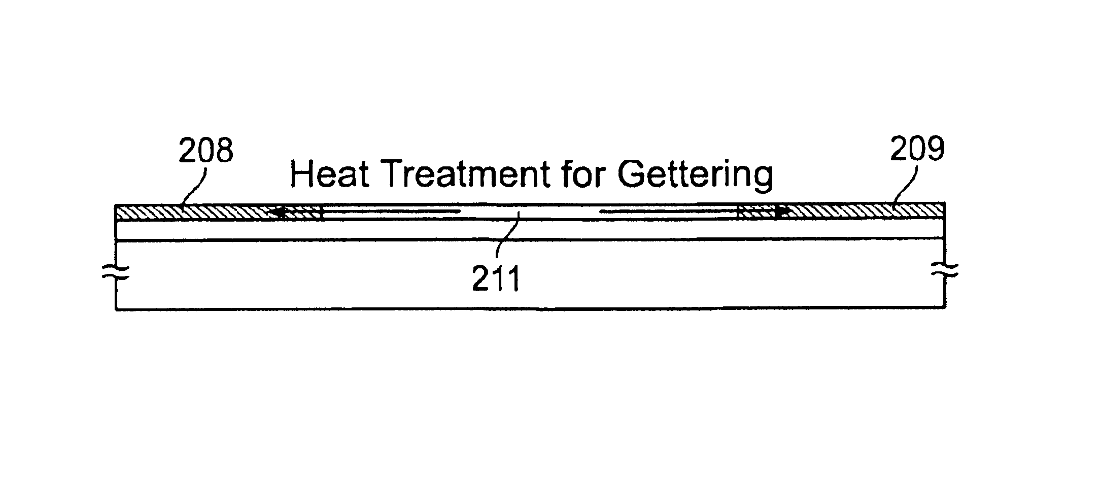
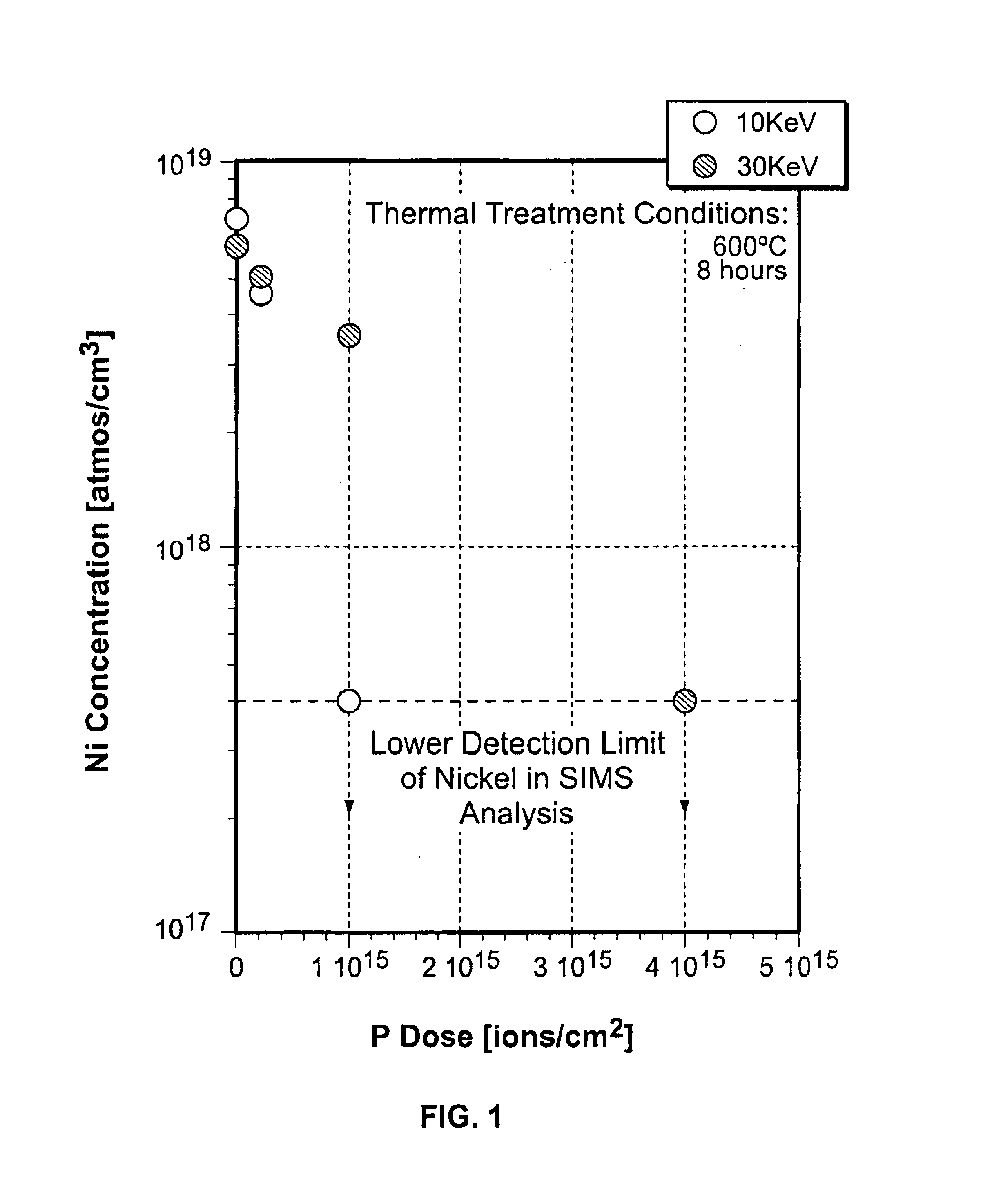
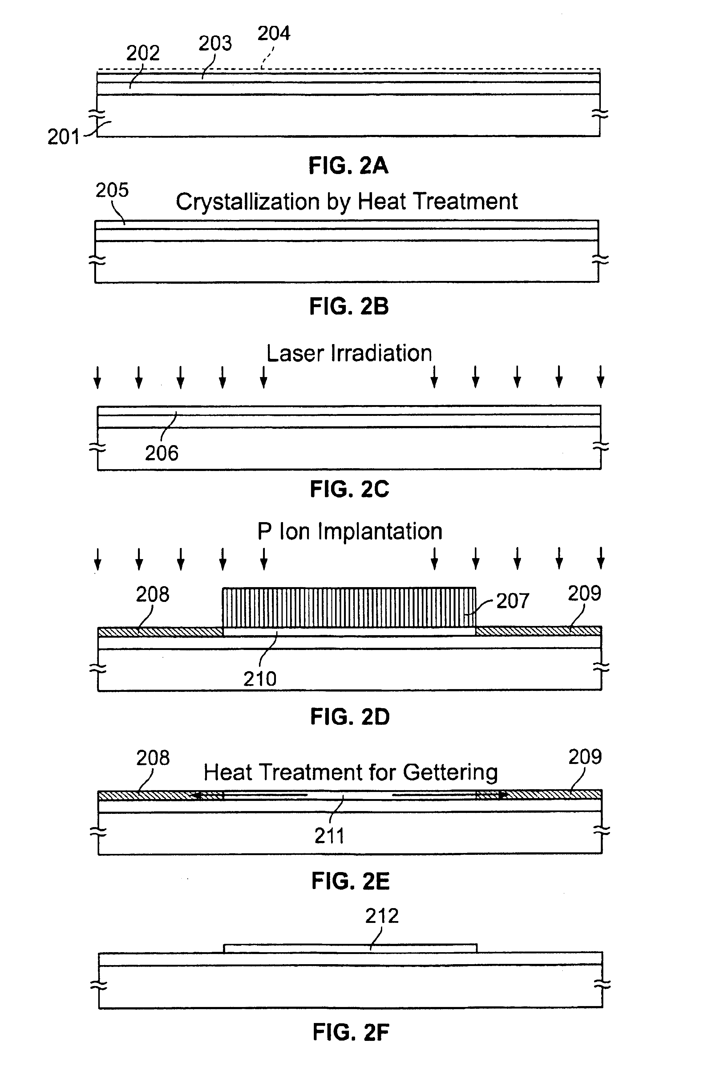
[0061]The present example describes a means in which P (phosphorus) is used for gettering nickel from a crystalline silicon film (polysilicon film) crystallized by using nickel as the catalyst element and the effect thereof.

[0062]Referring first to FIG. 2A, a 200 nm thick silicon oxide film 202 was formed as a base film by means of plasma CVD on a glass substrate 201. Then, a 50 nm thick amorphous silicon film 203 was formed by low pressure thermal CVD (or by plasma CVD). An amorphous silicon film formed at a thickness of from 10 to 75 nm (preferably from 15 to 45 nm) is sufficient.

[0063]Otherwise, an amorphous semiconductor film containing silicon, such as SixGe1-x (where 0

[0064]The crystallization of the amorphous silicon film 203 was performed thereafter. For the details of the process conditions, reference can be made to the description of Example 1 in Japanese Patent Application Laid-open No. Hei 8-130652.

[0065]Then,...

example 2

[0137]The present example describes an example of crystallizing an amorphous semiconductor film by a different method from Example 1 with reference to FIGS. 10A to 10F. The details of this crystallizing means may be referred to Example 2 described in Japanese Patent Application Laid-open No, Hei 7-130652.

[0138]Referring to FIG. 10A, reference numeral 301 denotes a glass substrate, and a base film 302 and a 50 nm-thick amorphous silicon film 303 were formed thereon. Then, a silicon oxide film was formed thereon as a mask insulating film 304, and an aperture portion 305 was provided therein to selectively add a catalyst element therethrough (nickel is used again in the present example).

[0139]Then, an ultra-thin oxide film (not shown) was formed on the surface of the exposed portion of the amorphous silicon film 303 by irradiating UV light under oxygen atmosphere. This oxide film functions to improve the wettability of the amorphous silicon film. Subsequently, a nickel acetate solution...

example 3

[0151]The present example refers to a process for manufacturing a CMOS circuit having an N-channel type TFT and a P-channel type TFT provided in a complementary structure.

[0152]Referring to FIG. 11A, reference numeral 11 denotes a glass substrate; 12, a base film; 13, an active layer of an N-channel type TFT; and 14, an active layer of a P-channel type. The active layers 13 and 14 may be formed by using, for example, the island-like pattern 212 shown in FIG. 2F.

[0153]Then, a 150 nm-thick silicon oxide film was formed by plasma CVD or low pressure thermal CVD to obtain a gate insulating film 15 (FIG. 11A).

[0154]A metal film containing aluminum as the principal component was formed thereafter (not shown), and was patterned to provide a prototype for the gate electrode to be used in the later steps. Then, the technique described by the present inventors in Japanese Patent Application Laid-open No. Hei 7-135318 was applied. Thus, porous anodic oxide films 16 and 17, as well as dense ano...


PUM

PropertyMeasurementUnit
temperatureaaaaaaaaaa
crystallization temperatureaaaaaaaaaa
temperatureaaaaaaaaaa

Abstract

A method of producing a semiconductor device which removes catalyst elements from a silicon-containing semiconductor film while maintaining the advantage of low temperature process is provided. The method comprises the steps of: forming an amorphous semiconductor film containing silicon on a glass substrate to crystallize it by using a catalyst element; selectively introducing into the amorphous semiconductor film an impurity belonging to Group 15 to form gettering regions and regions to be gettered; and causing the catalyst element in the silicon film to move to the gettering regions by heat treatment. Through the gettering process, the crystalline silicon film can be obtained in which the concentration of nickel contained therein is sufficiently reduced.

Description

BACKGROUND OF THE INVENTION[0001]1. Field of the Invention[0002]The present invention relates to a method of manufacturing a semiconductor device using a semiconductor thin film, and particularly to method of manufacturing a thin film transistor (TFT) using a crystalline semiconductor film containing silicon.[0003]Incidentally, the term “semiconductor device” used in the present specification includes all devices functioning by using a semiconductor, and not only a single element such as a TFT, but also an electro-optical device and application products furnished with the same are also included in the category of the semiconductor device.[0004]2. Description of the Related Art[0005]In recent years, a technique of constituting a semiconductor circuit by forming TFTs on a glass substrate and the like, has been rapidly developed. As such a semiconductor circuit, an electro-optical device such as an active matrix type liquid crystal display device is typical.[0006]The active matrix type...

Claims


Application Information

Patent Timeline
Patent Type & Authority Patents(United States)
IPC IPC(8): C30B25/04H01L21/336H01L21/02H01L21/20H01L29/66H01L29/786H01L21/322H01L21/77H01L21/84H01L27/12
CPCH01L21/2022H01L21/2026H01L21/3226H01L27/12H01L27/1277H01L29/66765H01L29/78675H01L29/78678H01L29/66757H01L21/02532H01L21/02422H01L21/02672H01L21/02686H01L21/00
Inventor OHNUMA, HIDETOYAMAZAKI, SHUNPEINAKAJIMA, SETSUOOHTANI, HISASHI
Owner SEMICON ENERGY LAB CO LTD
Why Eureka
Try Eureka