Image Forming Optical Element, Image Forming Optical Array, And Image Reading Device
- Summary
- Abstract
- Description
- Claims
- Application Information
AI Technical Summary
Benefits of technology
Problems solved by technology
Method used
Image
Examples
first embodiment
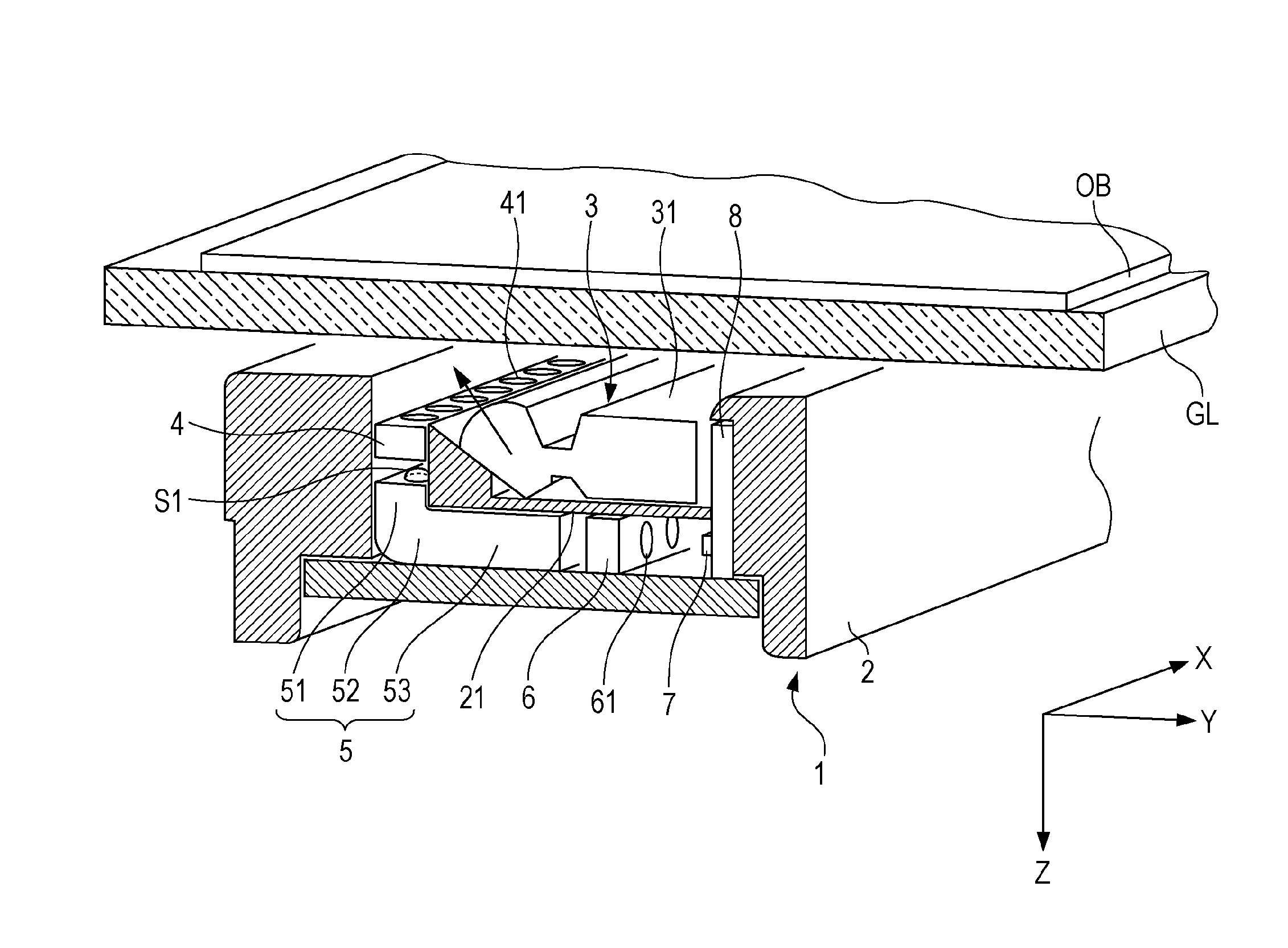
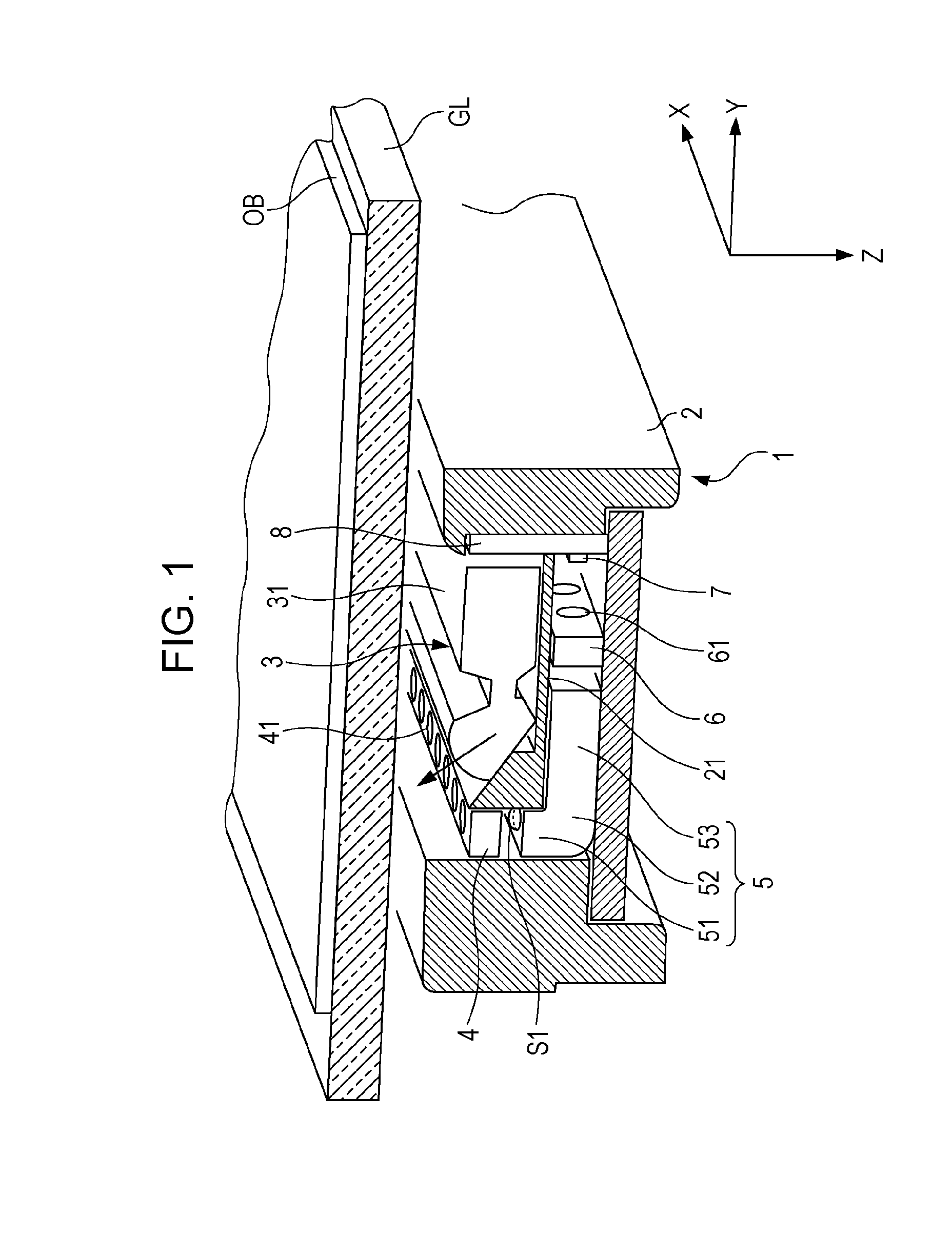
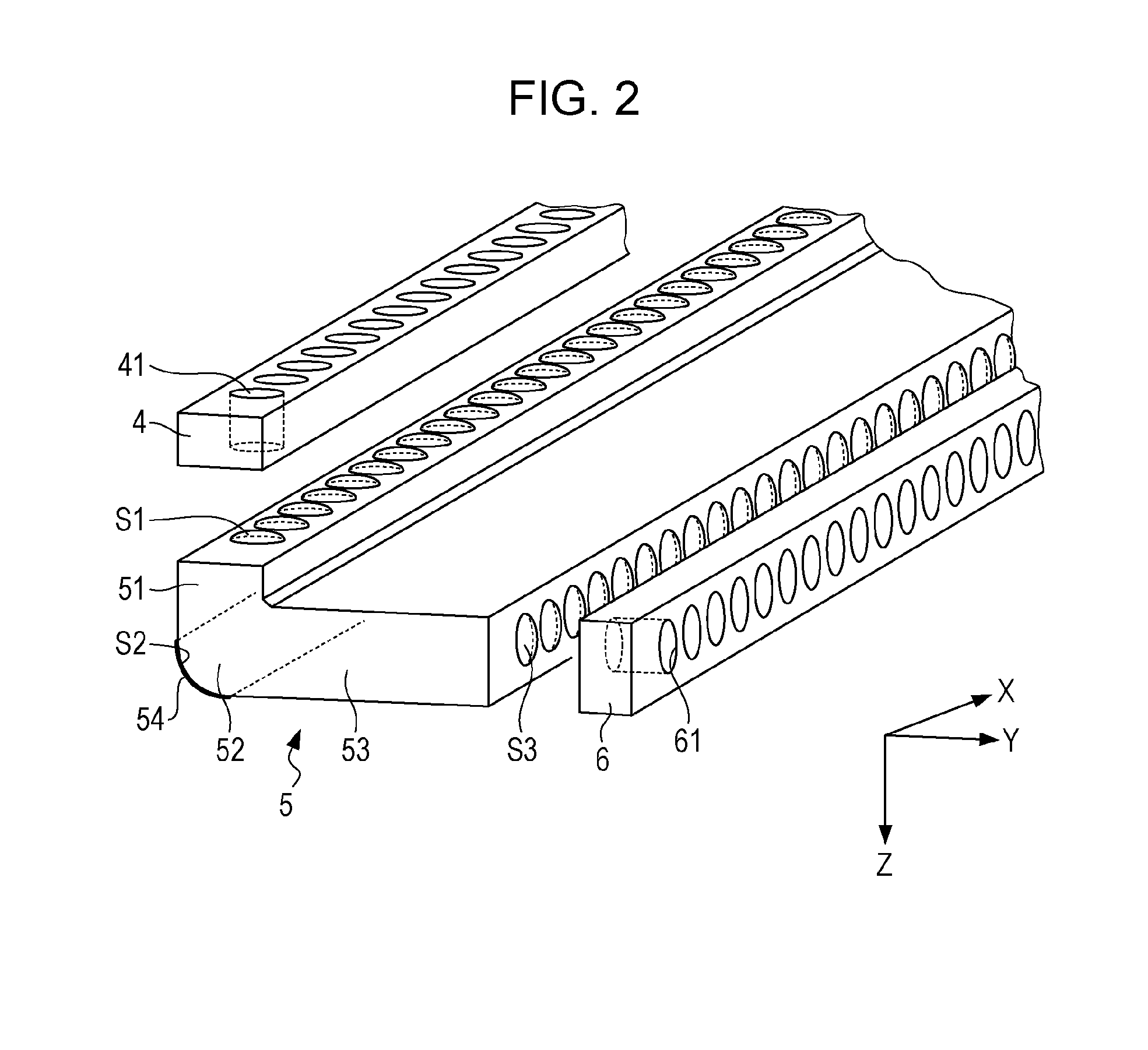
[0074]FIG. 1 is a partial cross-sectional perspective view illustrating a CIS module of an image reading device according to the invention. FIG. 2 is a perspective view illustrating an incident side aperture member, a lens array, and an output side aperture member in the CIS module shown in FIG. 1. The CIS module 1 is a device that reads an original document OB placed on an original document glass GL to read an image printed on the original document OB as a reading target, and is disposed just under the original document glass GL. The CIS module 1 has a rectangular frame 2 extending longer than a reading range of the original document OB in an X direction, and is provided with a light source unit 3, an incident side aperture member 4, a lens array 5, an output side aperture member 6, a sensor 7, and a printed circuit board 8 in the frame 2.
[0075]A separator 21 is disposed in the frame 2, and thus an internal space of the frame 2 is separated into an upper space for disposing the lig...
second embodiment
[0090]FIG. 3 is a partial cross-sectional perspective view illustrating the CIS module of the image reading device according to the invention. FIG. 4 is a perspective diagram illustrating the incident side aperture member, the lens array 5, and the output side aperture member in the CIS module shown in FIG. 3. The CIS module 1 is a device that reads an original document OB placed on an original document glass GL to read an image printed on the original document OB as a reading target, and is disposed just under the original document glass GL. The CIS module 1 has a rectangular frame 2 extending longer than a reading range of the original document OB in an X direction, and is provided with a light source unit 3, an incident side aperture member 4, a lens array 5, an output side aperture member 6, a sensor 7, and printed circuit boards 8A and 8B in the frame 2.
[0091]A separator 21 is disposed in the frame 2, and thus an internal space of the frame 2 is separated into an upper space fo...
third embodiment
[0120]First, FIG. 13 will be described. In the third embodiment, the connection unit 52 is formed of an incident unit 51 growing in the Z direction, left and right portions 55 curved from the lower end of the incident unit 51 and extending to the right side, and an output unit 53 curved from the right end of the left and right portions 55 and extending downward. That is, the connection unit 52 has a shape perpendicularly curved by a first curve portion CV1 from the incident unit 51 to the left and right portions 55 and perpendicularly curved by a second curve portion CV2 from the left and right portions 55 to the output unit 53.
[0121]On the upper face of the incident unit 51, a plurality of incident side lens faces S1 corresponding to, one-to-one, a plurality of through-holes 41 of the incident side aperture member 4 are formed in a line at a predetermined pitch in the X direction. On the lower face of the output unit 53 of the connection unit 52, a plurality of output side lens fac...
PUM
 Abstract
Description
Claims
Application Information


