
Method for electrical connection between two surfaces of ceramic substrate

a technology of ceramic substrate and electrical connection, which is applied in the direction of electrical equipment, printed circuits, line/current collector details, etc., can solve the problems of long electroplating duration, difficult control of quality, bottleneck of controlling yield rate, etc., to save lots of time, facilitate application in the production process, and enhance the convenience of manufacturing process

Inactive Publication Date: 2012-08-02
CHENMING MOLD IND CORP
View PDF1 Cites 1 Cited by
  • Summary
  • Abstract
  • Description
  • Claims
  • Application Information

AI Technical Summary

Benefits of technology

[0012]In the method for an electrical connection between two surfaces of a ceramic substrate in accordance with the present invention, the through hole is designed and disposed between the two surfaces of the ceramic substrate, and an electrically conductive element is fixed into the through hole and used as an electrical connection path for the circuits on both surfaces of the ceramic substrate. Such arrangement not only saves lots of time and enhances the convenience of the manufacturing process, but also overcomes the difficulties of the conventional ways of controlling the yield rate and facilitates the application in the production process. The technical characteristics of the present invention will become apparent with the detailed description of preferred embodiments and related drawings as follows.

Problems solved by technology

However, such method has to lengthen the duration for the electroplating and is laborious in the work during the actual manipulation as electrical characteristics are concerned, and the parameters including current, voltage, chemical concentration and operating temperature must be controlled accurately.
Furthermore, it is difficult to control the quality, and a void through hole which is not filled completely may result easily and causes a bottleneck of controlling the yield rate.

Method used


Image

  • Method for electrical connection between two surfaces of ceramic substrate
  • Method for electrical connection between two surfaces of ceramic substrate
  • Method for electrical connection between two surfaces of ceramic substrate

Examples


Embodiment Construction

[0017]To make it easier for our examiner to understand the technical characteristics, contents, advantages, and effects of the present invention, preferred embodiments together with related drawings are provided for describing and illustrating the invention. These preferred embodiments are provided for the purpose of illustration only, but not intended for limiting the scope of the invention.

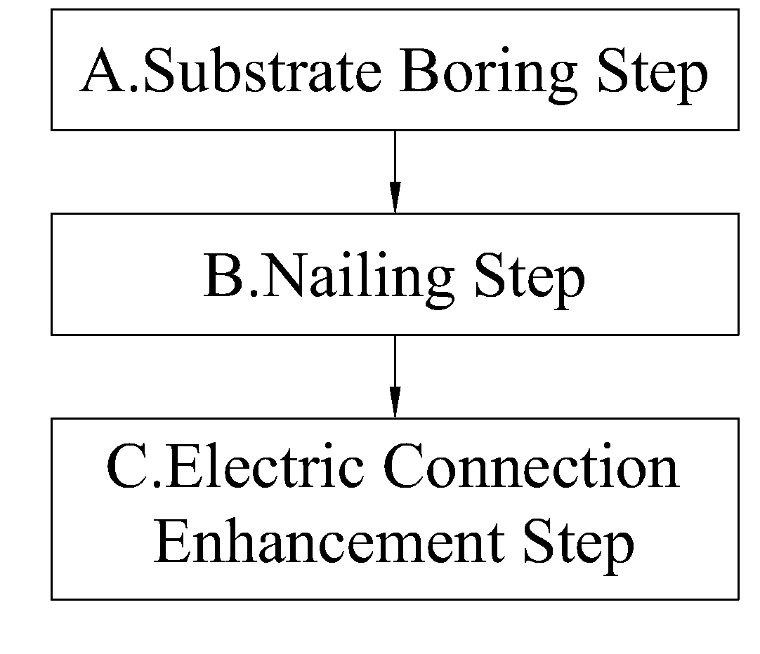
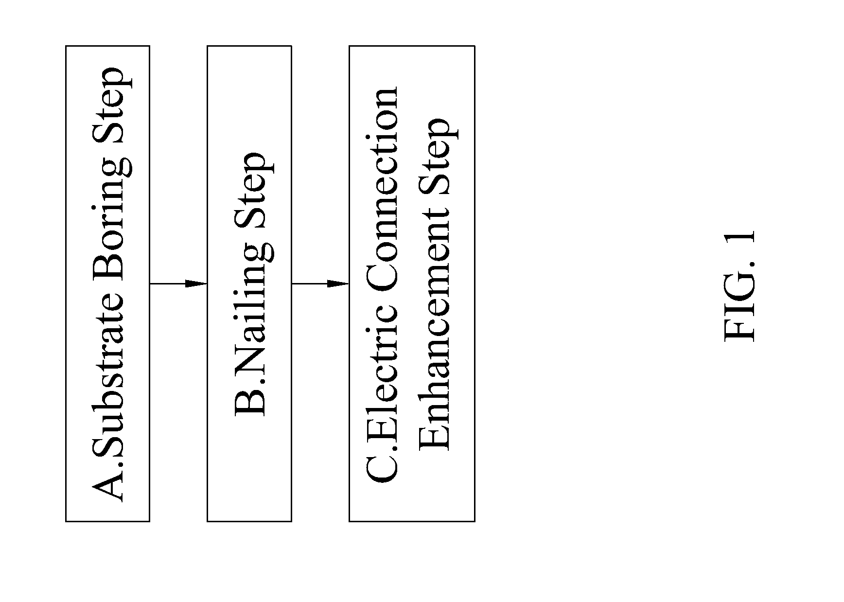
[0018]With reference to FIG. 1 for a method for an electrical connection between two surfaces of a ceramic substrate in accordance with a preferred embodiment of the present invention, the method comprises the following steps:

[0019]A. Substrate Boring Step;

[0020]B. Nailing Step; and

[0021]C. Electric Connection Enhancement Step.

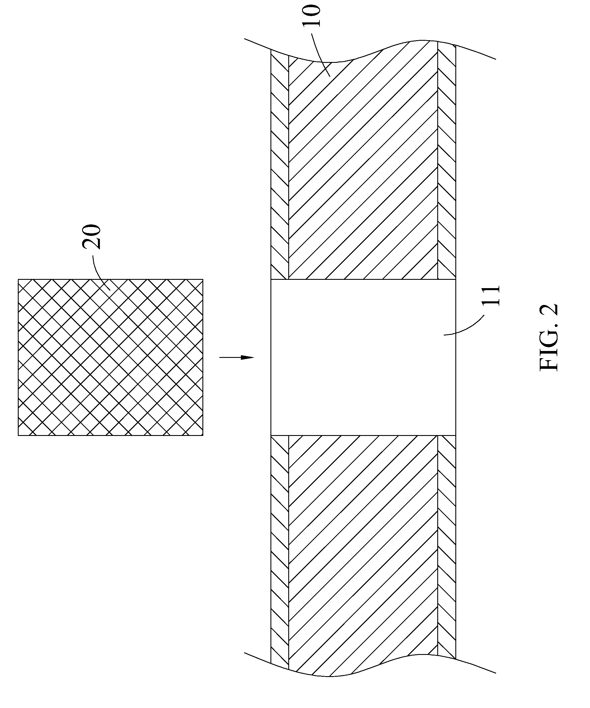
[0022]In FIG. 2, after the substrate boring step (Step A) takes place, a through hole is formed at electrical connection points on both surfaces of the ceramic substrate (10) by a tool after circuits are laid, such that a through hole (11) which can be a circular hole or a...


PUM

PropertyMeasurementUnit
Electrical conductivityaaaaaaaaaa
Flexibilityaaaaaaaaaa

Abstract

The present invention discloses a method for electrical connection between two surfaces of a ceramic substrate, and the method includes the steps of forming a through hole between the two surfaces of the ceramic substrate corresponding to electrical connection points of a circuit on the ceramic substrate, and then mounting a conductive assembly inside the through hole to form a conduction path between the two surfaces of the ceramic substrate. By this means, time cost of manufacturing of ceramic substrate circuit board could be largely decreased, and the manufacturing procedures could be much simplified as well.

Description

BACKGROUND OF THE INVENTION[0001]1. Field of the Invention[0002]The present invention relates to a method for an electrical connection between two surfaces of a ceramic substrate, and more particularly to a manufacturing process technology that uses a dry implanting nail as a means for an electrical connection between two surfaces of a substrate.[0003]2. Brief Description of Related Art[0004]At present, ceramic substrate used extensively in the electronic industry becomes an important board material for printed circuit boards. For example, the surface of an LED ceramic substrate is electroplated, such that both surfaces of the substrate can be used for circuit layout and configuration.[0005]In the conventional circuit manufacturing process of a ceramic substrate, it is necessary to connect separate circuit points on both surfaces of the substrate or perform a thermal conduction treatment between both surfaces of the substrate. Since it is not easy to lay the circuit to the periphery...

Claims


Application Information

Patent Timeline
IPC IPC(8): H01R43/00
CPCH05K1/0306H05K3/0047Y10T29/49117H05K2201/10242H05K3/4046
Inventor CHIOU, YAU-HUNGFAN, SHU-HUIKAO, MING-TZE
Owner CHENMING MOLD IND CORP
Learn More