Imaging Optical Array And Image Reading Device

a technology of optical array and image reading device, which is applied in the field of imaging optical array, can solve the problems of crosstalk between adjacent imaging optical elements, inability to properly display the function of light shielding members, and inability to erect equal-magnification images of objects to be read

Inactive Publication Date: 2012-08-09
SEIKO EPSON CORP
View PDF6 Cites 4 Cited by
  • Summary
  • Abstract
  • Description
  • Claims
  • Application Information

AI Technical Summary

Benefits of technology

[0010]An advantage of some aspects of the invention is to provide a technology capable of allowing a function of a light shielding member to be appropriately exhibited by stabilizing the positional relationship between imaging optical elements and light shielding member.

Problems solved by technology

When the light, which is incident to another imaging optical element due to the crosstalk, is imaged on this imaging optical element, there is a concern that an erect equal-magnification image of the object to be read may not be appropriately formed.
Therefore, there is a concern that an error in a positional alignment between the imaging optical elements and the light shielding member may occur at the time of assembling the imaging optical array, or the positional relationship between the imaging optical elements and the light shielding member may be deviated due to thermal distortion or the like in the imaging optical elements and the light shielding member, which is caused by a temperature variation after assembly, and thereby a function of the light shielding member may not be exhibited appropriately.
However, in this imaging optical array, crosstalk between adjacent imaging optical elements becomes a problem.

Method used


Image

  • Imaging Optical Array And Image Reading Device
  • Imaging Optical Array And Image Reading Device
  • Imaging Optical Array And Image Reading Device

Examples


first embodiment

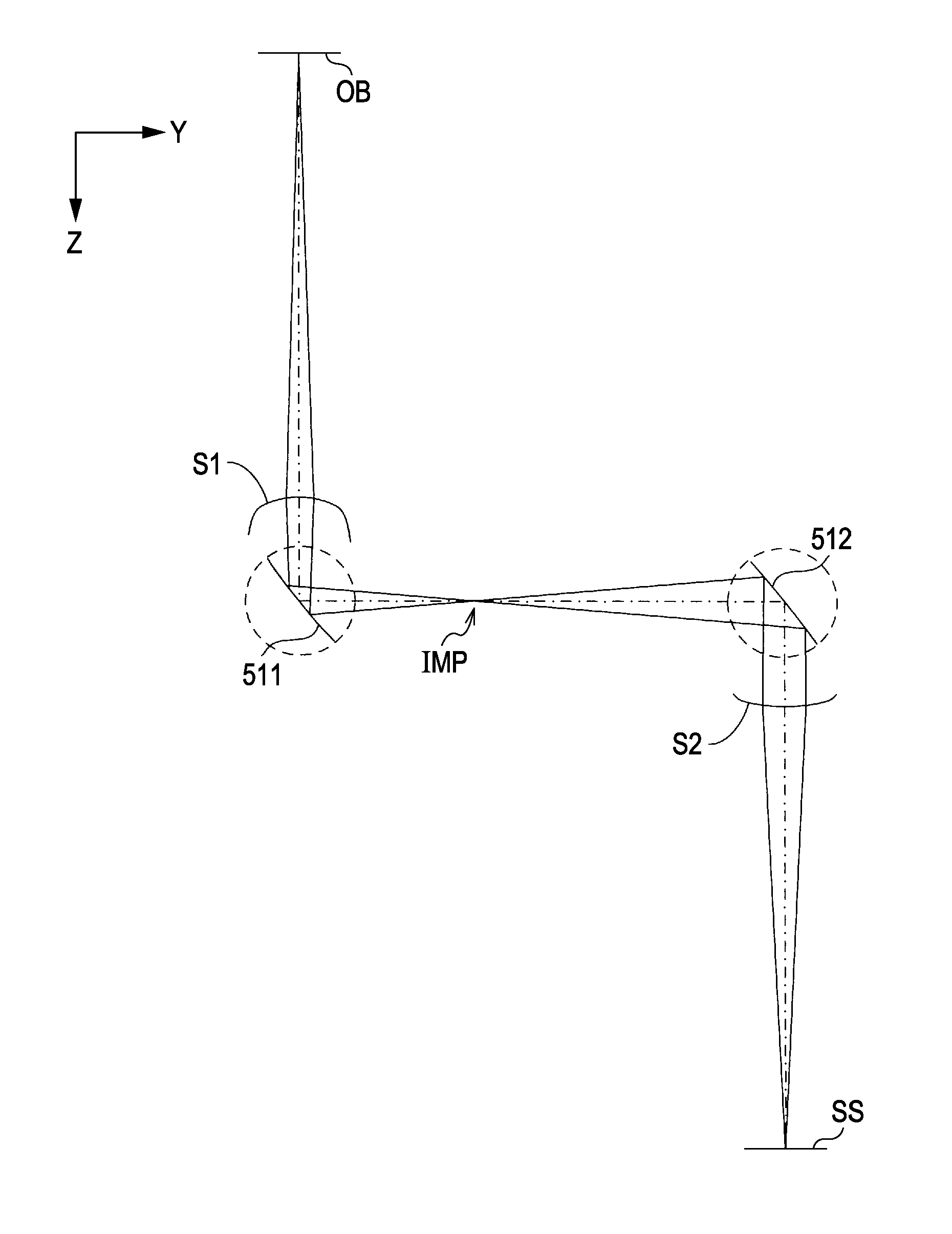
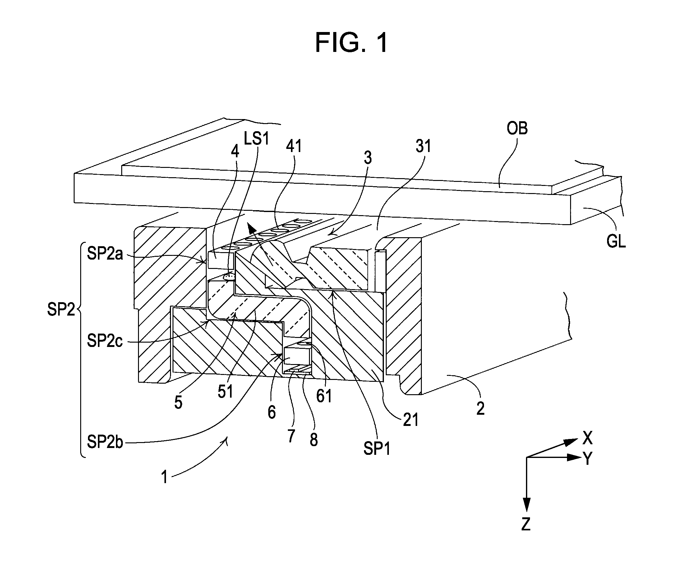
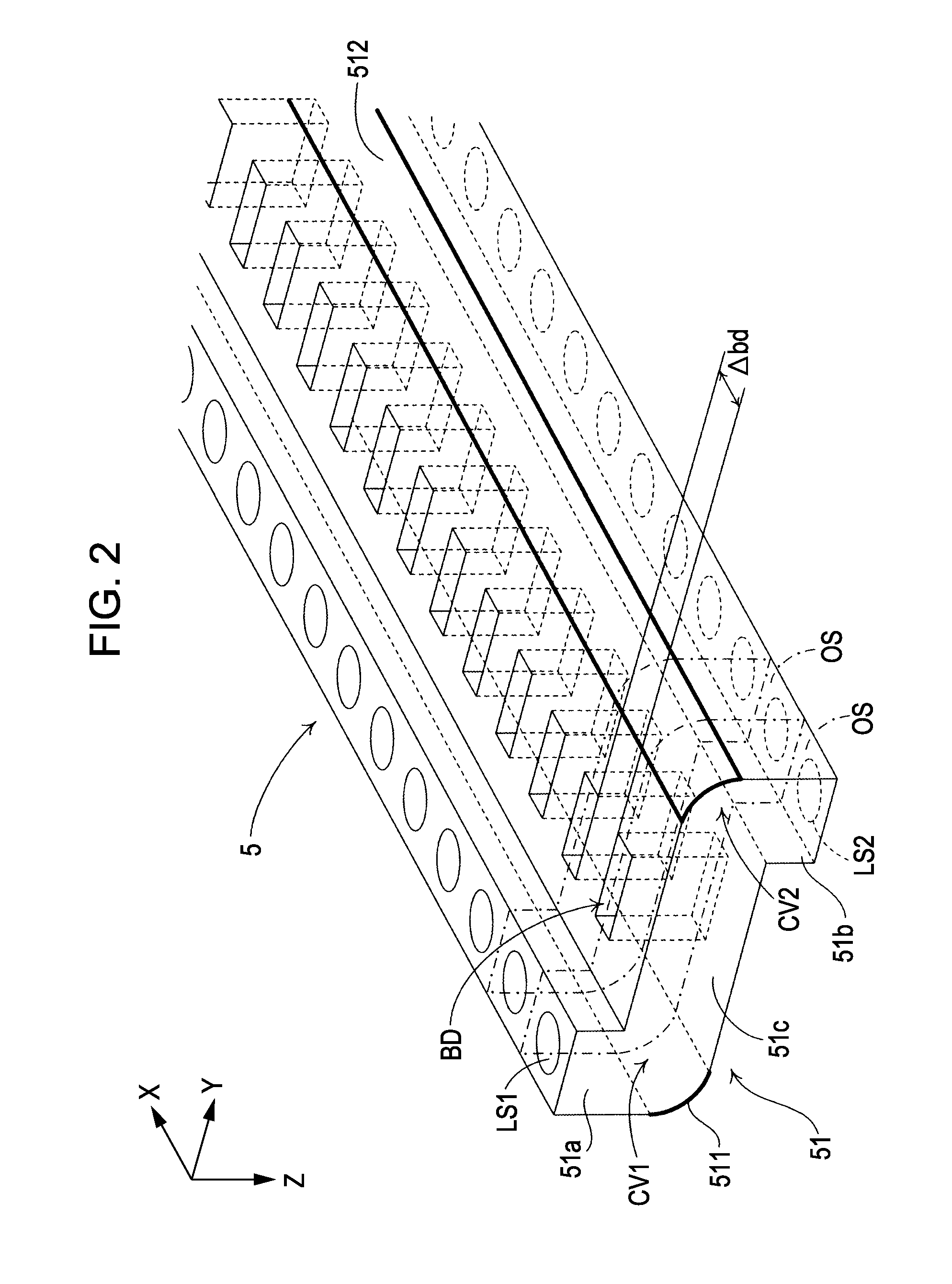
[0028]FIG. 1 shows a partial cross-sectional perspective view illustrating a schematic configuration of a CIS module that is an example of an image reading device according to the invention. FIG. 2 shows a perspective view illustrating a configuration of a lens array according to a first embodiment. In FIG. 1, FIG. 2, and in the following description, XYZ orthogonal coordinates are appropriately shown to illustrate the positional relationship of each member. In addition, arrow sides in the coordinate axes are set as positive sides, and opposite sides of the arrow sides in the coordinate axes are set as negative sides. Furthermore, in the following description, the negative side of the Z-direction is regarded as the upper side, the positive side of the Z-direction is regarded as the lower side, the negative side of the Y-direction is regarded as the left side, the positive side of the Y-direction is regarded as the right side, the negative side of the X-direction is regarded as the f...

second embodiment

[0047]The first embodiment and this second embodiment are different from each other in that whether or not a concave portion CP is formed at both ends of the lens array 5 in the X-direction. Therefore, in the following description, this difference will be mainly described, and corresponding reference numerals will be given to common portions, and description thereof will be appropriately omitted. In addition, since the second embodiment has the same configuration as the first embodiment, it is needless to say that the same effect as the first embodiment can be obtained in the second embodiment.

[0048]In the first embodiment, the void BD is formed between the imaging optical elements OS adjacent to each other in the X-direction. Therefore, the void BD is disposed at both sides of the imaging optical elements OS in the X-direction, respectively, such that light that passes through between the voids BD is supplied for the imaging by the imaging optical elements OS. That is, it may be as...

third embodiment

[0051]In the above-described embodiments, the void BD is formed as a penetration hole that vertically penetrates the lens array 5 (transparent medium). However, an aspect of the void BD is not limited to this, and may have a configuration shown in FIG. 6. Here, FIG. 6 shows a perspective view illustrating a configuration of a lens array according to a third embodiment. That is, as shown in FIG. 6, in the third embodiment, the void BD is a void having the bottom, which is empty from an upper external side of the light guiding portion 51 (horizontal portion 51c) of the lens array 5 (transparent medium) to a position between the imaging optical elements OS adjacent to each other in the X-direction.

[0052]In addition, the main difference between the third embodiment and the above-described embodiments is an aspect of the void BD. Therefore, in the following description, this difference will be mainly described, and corresponding reference numerals will be given to common portions, and de...


PUM


Abstract

An imaging optical array includes a plurality of imaging optical elements, which is arranged in a line in an arrangement direction, each including incidence lens to which light from an object is incident, an emission lens that emits light, and a light guiding portion that connects the incidence lens and the emission lens and that guides the light incident from the incidence lens to the emission lens, and which images an erect equal-magnification image of an object by the incidence lens and the emission lens, in which the plurality of imaging optical elements is integrally formed of a transparent medium in a state where the respective light guiding portions of the plurality of imaging optical elements are arranged in a line in the arrangement direction, and a void between the light guiding portions of the imaging optical elements adjacent to each other is empty in the transparent medium.

Description

CROSS REFERENCE TO RELATED APPLICATION[0001]The present invention contains subject matter related to Japanese Patent Application No. 2011-022526 filed in the Japanese Patent Office on Feb. 4, 2011, the entire contents of which are incorporated herein by reference.BACKGROUND[0002]1. Technical Field[0003]The present invention relates to an imaging optical array in which a plurality of imaging optical elements, which forms an erect equal-magnification image of an object, is arranged in a line, and an image reading device that reads an image of an object using the imaging optical array.[0004]2. Related Art[0005]In an image scanner, a facsimile, a copying machine, a banking terminal device, or the like, a contact image sensor module (hereinafter, abbreviated as a “CIS module”) is used as an image reading device. This CIS module reads an image of an object to be read by irradiating with light the object to be read and detecting light that is emitted from the object to be read at this time...

Claims


Application Information

Patent Timeline
Patent Type & Authority Applications(United States)
IPC IPC(8): H04N1/04
CPCH04N1/0306H04N1/0312H04N1/0315H04N2201/02479H04N2201/02456H04N2201/02458H04N2201/02462H04N1/0318
Inventor TAKEDA, TAKASHIKINOSHITA, SATOSHI
Owner SEIKO EPSON CORP
Why Eureka
Try Eureka