Variable gain amplifier circuit

a gain amplifier and variable gain technology, applied in amplifiers, amplifiers with semiconductor devices/discharge tubes, amplifiers, etc., can solve the problems of large apparatus size, inability to achieve desired gain, and attenuation of input signal level, so as to achieve high accuracy gain adjustment, suppress the effect of input impedance change caused by gain chang

Active Publication Date: 2012-08-16
LAPIS SEMICON CO LTD
View PDF3 Cites 0 Cited by
  • Summary
  • Abstract
  • Description
  • Claims
  • Application Information

AI Technical Summary

Benefits of technology

[0011]An object of the present invention is to provide a variable gain amplifier circuit with a small-sized configuration that can accurately adjust the gain without causing a transmission loss of an input signal.
[0014]In this configuration, a switching device for setting an amplification transistor to a deactivated state does not exist in the input signal line. Accordingly, attenuation of the input signal level, which is caused by the on resistance and parasitic capacitance of the switching device, can be prevented. As the input signal line is directly connected to the input signal terminal of each amplification transistor, changes in the input impedance caused by gain changes can be suppressed. As the error between the actual gain at the time of amplification by the amplification transistor and the designed gain can be thereby minimized, highly accurate gain adjustment can be performed.

Problems solved by technology

One problem of this variable gain amplifier circuit is attenuation of a signal level.
Another problem is that a desired gain cannot be achieved.
Another problem is a large size of the apparatus as such a two-input selector is provided for each amplification transistor.Patent Literature 1: Japanese Patent Kokai No. 2010-239401

Method used


Image

  • Variable gain amplifier circuit
  • Variable gain amplifier circuit
  • Variable gain amplifier circuit

Examples


Embodiment Construction

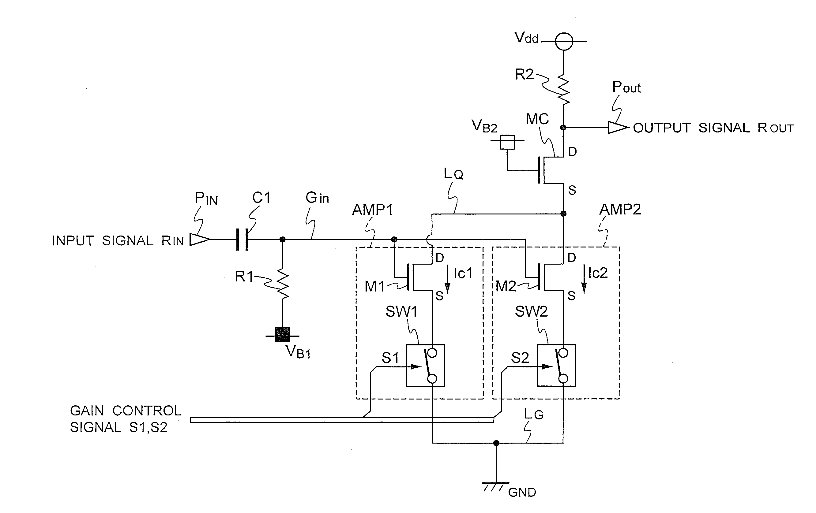
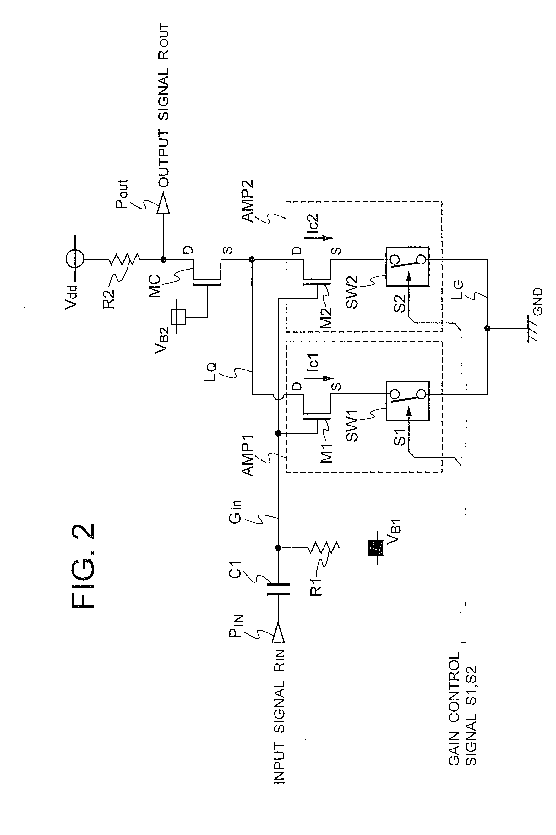
[0019]In the variable gain amplifier circuit according to the present invention, a plurality of amplification portions are connected with each other in parallel between an amplification coupling line and a grounding line. The amplification portion includes a switching device and an amplification transistor, which induces a current corresponding to an input signal to flow between the amplification coupling line and the grounding line via the switching device when the switching device is in the on state. The amplitude gain is varied by, according to a gain control signal, separately switching on or off the switching devices of the respective amplification portions.

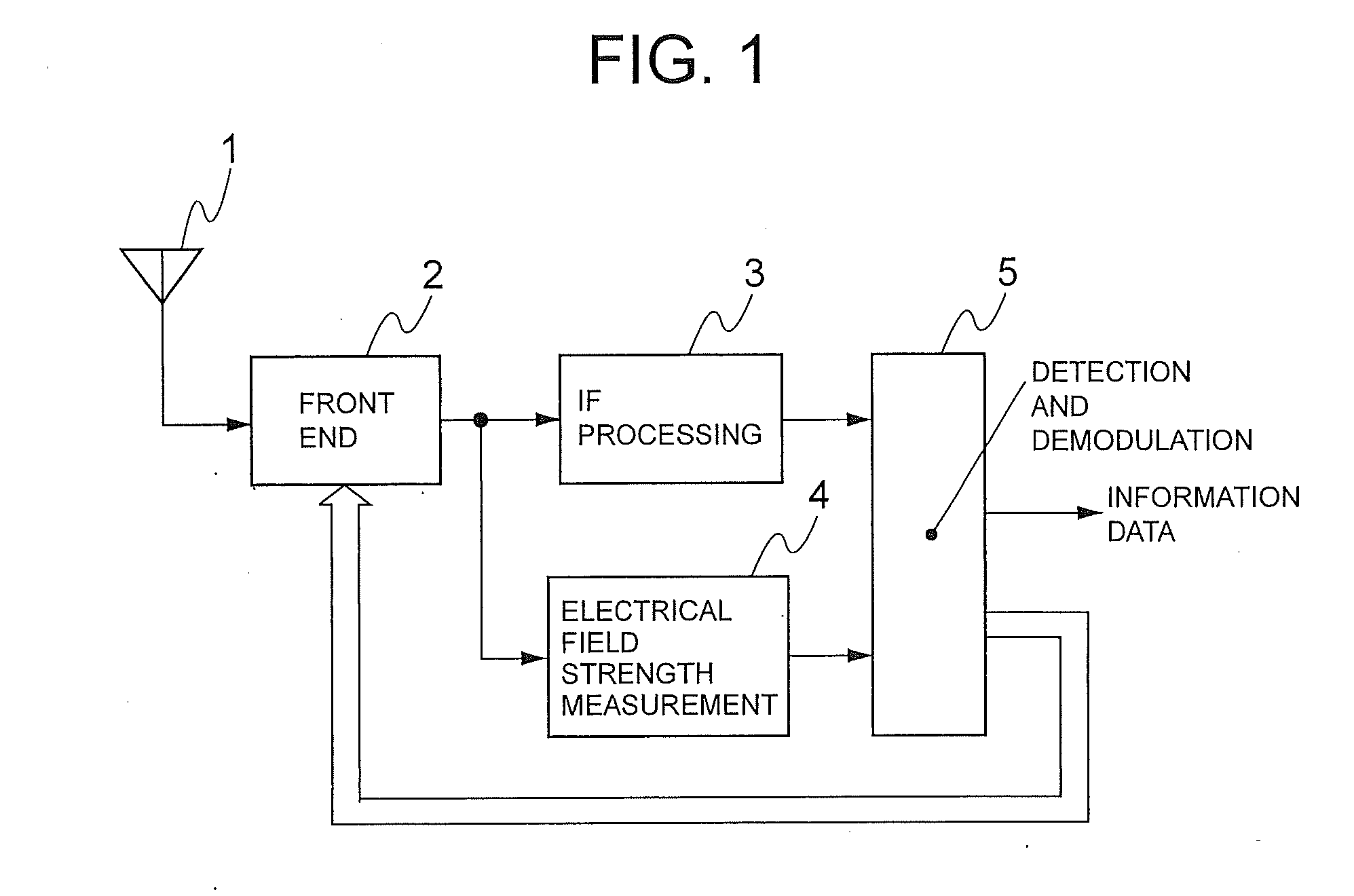
[0020]FIG. 1 is a block diagram illustrating a general configuration of a wireless receiver including a variable gain amplifier circuit according to the present invention.

[0021]In FIG. 1, a front end 2 amplifies a received signal received by an antenna 1, converts the signal into an intermediate frequency signal, and supplie...


PUM


Abstract

A variable gain amplifier circuit with a small-sized configuration can accurately adjust the gain without causing a transmission loss of an input signal. A plurality of amplification portions are connected with each other between an amplification coupling line and a grounding line in parallel. The amplification portion includes a switching device and an amplification transistor, which induces a current corresponding to an input signal to flow between the amplification coupling line and the grounding line via the switching device when the switching device is in the on state. The amplitude gain is varied by, according to a gain control signal, separately switching on and off the switching devices of the respective amplification portions.

Description

BACKGROUND OF THE INVENTION[0001]1. Technical Field[0002]The present invention relates to a variable gain amplifier circuit that amplifies an input signal at variable gain.[0003]2. Description of the Related Art[0004]A receiver used in wireless mobile communications is, at its front end, provided with a variable gain amplifier circuit that varies a gain according to the level of a received signal in order to maintain the level of the received signal at a constant level even when radio attenuation is caused by, for example, the distance between the receiver and the base station and existence of an obstacle therebetween.[0005]A variable gain amplifier circuit with a wider variable gain range is proposed (see FIG. 1 of Patent Literature 1). In the configuration of this circuit, collector terminals of a plurality of amplification transistors (Q1 to Qn), i.e., transistors that amplify a received signal, are connected with each other.[0006]The base terminals of the amplification transisto...

Claims


Application Information

Patent Timeline
Patent Type & Authority Applications(United States)
IPC IPC(8): H03G3/20
CPCH03G1/0088H03G1/0029
Inventor TAKAGI, KATSUYUKI
Owner LAPIS SEMICON CO LTD
Why Eureka
Try Eureka