Electroluminescent display device with optically communicating chiplets

a technology of optical communication and display device, which is applied in the direction of semiconductor devices, identification means, instruments, etc., can solve the problems of low performance of thin-film transistors made from amorphous or polycrystalline silicon, low performance of conventional transistors made from crystalline silicon wafers, and inability to meet the requirements of the application, so as to improve communication, reduce latency, and increase bandwidth

Active Publication Date: 2012-08-23
GLOBAL OLED TECH
View PDF22 Cites 63 Cited by
  • Summary
  • Abstract
  • Description
  • Claims
  • Application Information

AI Technical Summary

Benefits of technology

[0020]The present invention has the advantage that it improves the communication between a plurality of control elements in a flat-panel substrate. Optical distribution removes delays experienced by electrical communications methods, including transmission-line and RLC delays. The present invention therefore provides communications with increased bandwidth and reduced latency. Wavelength-division multiplexing can be used to further increase bandwidth. Transmitting light through the display backplane or a waveguide does not objectionably increase the volume occupied by the display. Forming light detectors and emitters on the chiplets permits the use of high-density lithography to form effective optical circuits on the chiplets. The present invention does not increase manufacturing cost of the substrate as do prior art methods of substrate light-piping. The present invention provides robust communications between chiplets, which communication can be interrupted only by breaking the substrate.

Problems solved by technology

Thin-film transistors made from amorphous or polycrystalline silicon are relatively larger and have lower performance than conventional transistors made from crystalline silicon wafers.
Moreover, such thin-film devices typically exhibit local or large-area non-uniformity that results in perceptible non-uniformity in a display employing such materials, and the manufacturing processes are expensive.
Such control signals are limited in bandwidth because of the length of the wires, the wire conductivity, and the arrangement of the wires.
For large displays of high resolution, such communication bandwidth restrictions can limit the refresh rate of the display, the resolution, or the accuracy and precision of the display signals.
However, these disclosures do not provide improved communication between pixel control elements in a flat-panel display.
These schemes are not applicable to display devices, in which the substrate viewed by the user cannot be obscured by a stacked substrate or other component.
This scheme does not provide communication between active-matrix control elements, and depends on objects external to the display to reflect light.
It does not address the need to improve communication between active-matrix control elements.

Method used


Image

  • Electroluminescent display device with optically communicating chiplets
  • Electroluminescent display device with optically communicating chiplets
  • Electroluminescent display device with optically communicating chiplets

Examples


Embodiment Construction

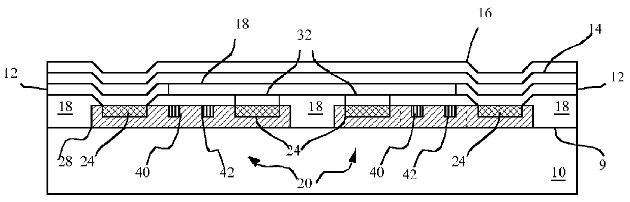
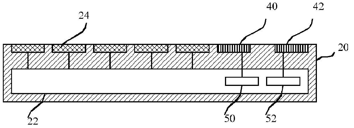
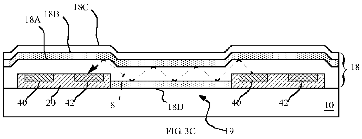
[0028]Referring to FIGS. 1 and 2, an electroluminescent display has a display substrate 10 having a device side 9 and a display area 11 (shown in FIG. 4). A plurality of patterned first electrodes 12 are formed over the display substrate 10 device side 9 in the display area, one or more layers 14 of light-emitting material are formed over the plurality of first electrodes 12, and at least one second electrode 16 is formed over the one or more layers 14 of light-emitting material, the first and second electrodes 12, 16 providing current to cause the layer 14 of light-emitting material to emit light in a light-emitting area within the display area. A plurality of chiplets 20 are adhered to the substrate 10, each chiplet 20 having: a chiplet substrate 28 separate and independent from the display substrate 10 located over, and adhered to, the device substrate 10 device side 9 in the display area; one or more connection pads 24; and a chiplet circuit 22 formed in the chiplet 20, the chip...


PUM


Abstract

An electroluminescent display includes a display substrate, a plurality of patterned first electrodes formed over the display substrate, one or more layers of light-emitting material formed over the plurality of first electrodes, at least one second electrode formed over the one or more layers of light-emitting material, and a plurality of chiplets. Each chiplet is electrically connected to a first electrode. Each chiplet further includes a light detector and a light emitter separate from the one-or-more layers of light-emitting material connected to the chiplet circuitry. The chiplet circuitry includes a modulating circuit for modulating light emitted by the light emitter and a demodulating circuit for demodulating light detected by the light detector so that light emitted by the light emitter of a first chiplet is received by the light detector of a second chiplet.

Description

CROSS REFERENCE TO RELATED APPLICATION[0001]Reference is made to commonly-assigned co-pending U.S. patent application Ser. No. 12 / 549,416, filed Sep. 28, 2009, entitled “CHIPLET DISPLAY WITH OPTICAL CONTROL”, the disclosures of which are incorporated by reference herein.FIELD OF THE INVENTION[0002]The present invention relates to display devices having a substrate with distributed, independent chiplet control elements.BACKGROUND OF THE INVENTION[0003]Flat-panel display devices are widely used in conjunction with computing devices, in portable devices, and for entertainment devices such as televisions. Such displays typically employ a plurality of pixels distributed over a substrate to display images. Each pixel incorporates several, differently colored light-emitting elements commonly referred to as sub-pixels, typically emitting red, green, and blue light, to represent each image element. Pixels and sub-pixels are not distinguished herein; all light-emitting elements are called pix...

Claims


Application Information

Patent Timeline
Patent Type & Authority Applications(United States)
IPC IPC(8): G09G5/00G09G3/30
CPCG09G3/2085G09G3/30G09G2300/0426G09G2360/142G09G2360/148G09G2370/18H01L2924/0002H01L25/167H01L27/1446H01L27/3255H01L2924/00H10K59/129G09F9/30
Inventor WHITE, CHRISTOPHER J.COK, RONALD S.HAMER, JOHN W.ARNOLD, ANDREW
Owner GLOBAL OLED TECH
Why Eureka
Try Eureka