Wiring substrate and method for manufacturing wiring substrates

a wiring substrate and manufacturing method technology, applied in the direction of cable/conductor manufacturing, semiconductor/solid-state device details, coatings, etc., can solve the problems of reducing the thickness of the entire wiring substrate, reducing the drop impact resistance, and osp film being prone to oxidization and discoloration

Active Publication Date: 2012-09-06
SHINKO ELECTRIC IND CO LTD
View PDF8 Cites 47 Cited by
  • Summary
  • Abstract
  • Description
  • Claims
  • Application Information

AI Technical Summary

Problems solved by technology

Consequently, there have been limits on the extent to which the thickness of the entire wiring substrate can be reduced.
This decreases the drop impact resistance.
However, since no Ni is present, the OSP film is prone to oxidization and discoloration.

Method used


Image

  • Wiring substrate and method for manufacturing wiring substrates
  • Wiring substrate and method for manufacturing wiring substrates
  • Wiring substrate and method for manufacturing wiring substrates

Examples


first embodiment

[0032]A first embodiment will now be described with reference to FIGS. 1 to 9.

[0033][Wiring Substrate]

[0034]First, the structure of the wiring substrate 1 will be described.

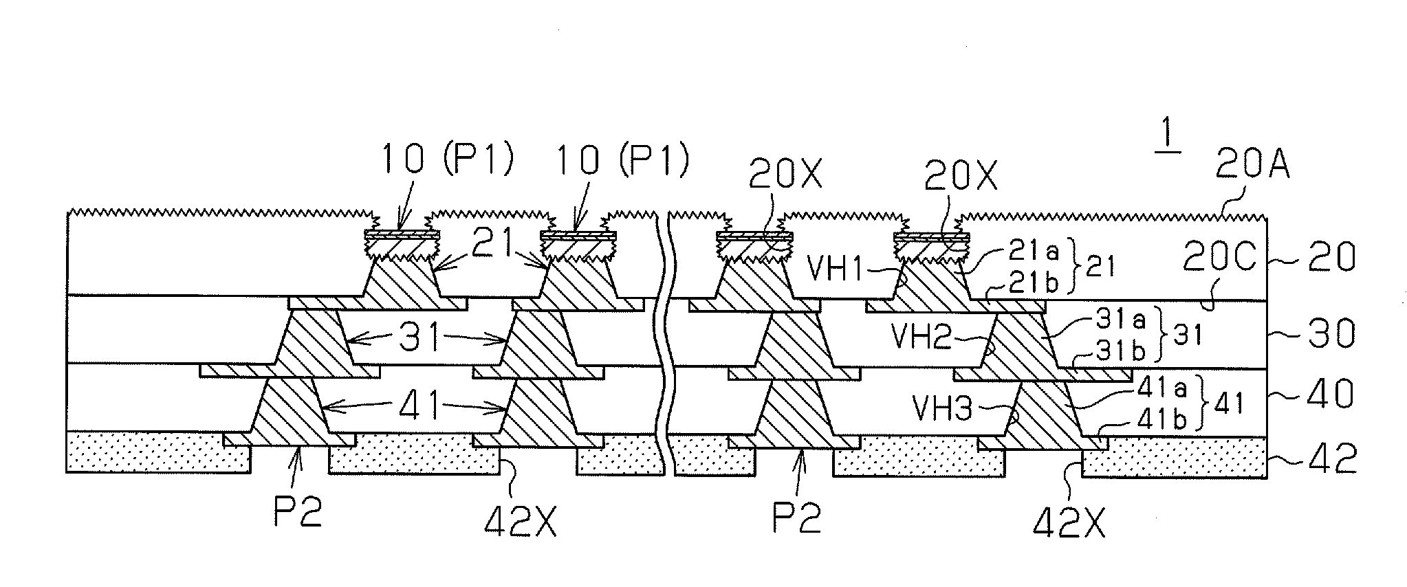
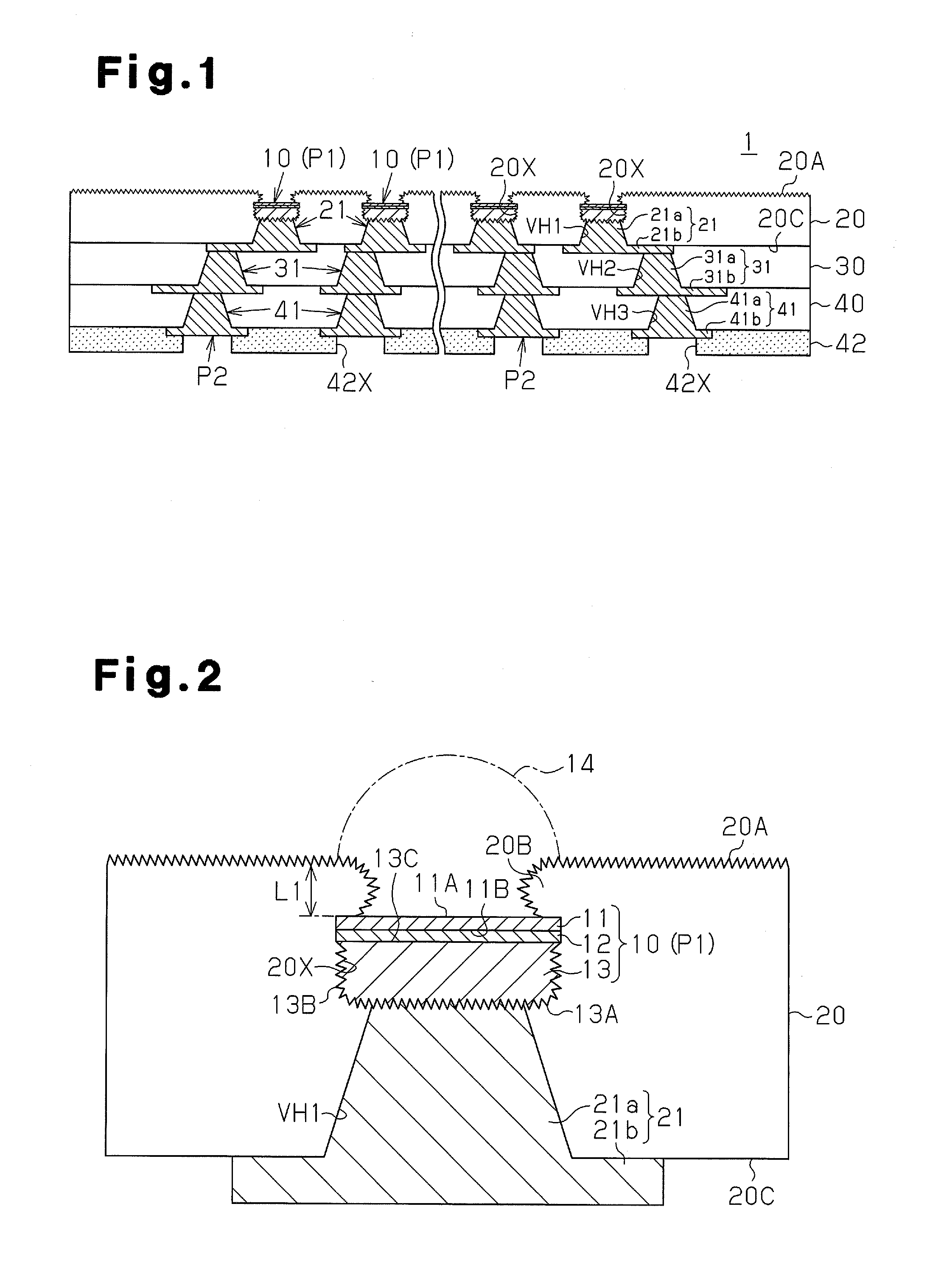
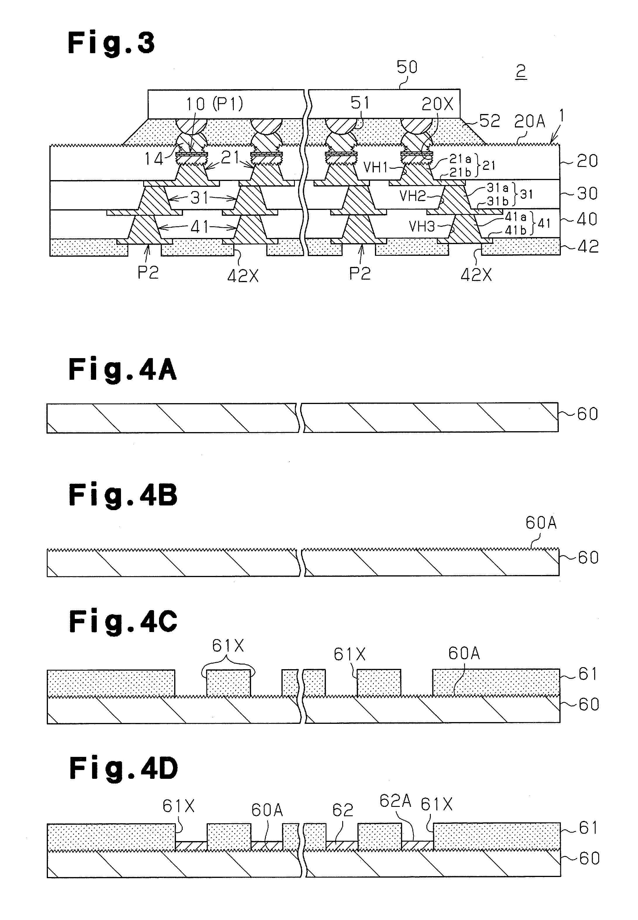
[0035]As illustrated in FIG. 1, the wiring substrate 1 includes first to fourth wiring layers 10, 21, 31, and 41 that are laminated with first to third insulating layers 20, 30, and 40 located in between. Via holes VH1, VH2, and VH3 filled with vias 21a, 31a, and 41a are formed in the insulating layers 20, 30, and 40, respectively. In this manner, the wiring substrate 1 of the present embodiment has the form of a “coreless substrate” and does not include a supporting base material. This differs from a wiring substrate manufactured through a typical build-up process in which a wiring substrate includes a desired number of build-up layers sequentially formed on one side or two sides of a core substrate, which serves as a supporting base material.

[0036]As the material of the second to fourth wiring layers 21, 31, an...

second embodiment

[0087]A second embodiment will now be described with reference to FIGS. 10 to 15. Like or same reference numerals are given to those components that are the same as the corresponding components illustrated in FIGS. 1 to 9. Such components will not be described in detail.

[0088][Wiring Substrate]

[0089]First, the structure of the wiring substrate 3 will be described.

[0090]As illustrated in FIG. 10, the wiring substrate 3 includes first to fourth wiring layers 10, 21, 31, and 41 that are laminated with first to third insulating layers 70, 30, and 40 in between. Via holes VH1, VH2, and VH3 are formed in the insulating layers 70, 30, and 40 and filled with vias 21a, 31a, and 41a. Like the wiring substrate 1 of the first embodiment, the wiring substrate 3 of the present embodiment is a “coreless substrate” that does not include a supporting base material.

[0091]Recesses 70X, which expose the pads P3, are formed on a first insulating layer 70, which is the outermost layer on one side of the ...


PUM


Abstract

A wiring substrate includes a wiring layer, an outermost insulating layer laminated to the wiring layer, and a pad electrically connected to the wiring layer and exposed from a surface of the outermost insulating layer. The pad consists essentially of a first metal layer and a second metal layer. The first metal layer includes a first surface, which is exposed from the surface of the outermost insulating layer, and a second surface, which is located opposite to the first surface. The second metal layer includes is formed between the second surface of the first metal layer and the wiring layer. The first metal layer is formed from a metal selected from gold or silver or from an alloy including at least one of gold and silver. The second metal layer is formed from palladium or a palladium alloy.

Description

CROSS-REFERENCE TO RELATED APPLICATIONS[0001]This application is based upon and claims the benefit of priority from prior Japanese Patent Application No. 2011-048021, filed on Mar. 4, 2011, the entire contents of which are incorporated herein by reference.BACKGROUND OF THE INVENTION[0002]The present invention relates to a wiring substrate and a method for manufacturing a wiring substrate.[0003]In the prior art, in order to achieve a high density wiring pattern for a wiring substrate used in a semiconductor package or the like, a build-up wiring substrate is known in which a build-up wiring layer and an insulating layer are laminated on upper and lower surfaces of a core substrate.[0004]The density of semiconductor chips mounted on build-up wiring substrates have become high. Thus, there is a demand for build-up wiring substrates that further increase the wiring pattern density and reduce the substrate thickness. In a build-up wiring substrate, the layered portion of a wiring layer a...

Claims


Application Information

Patent Timeline
Patent Type & Authority Applications(United States)
IPC IPC(8): H05K1/09B05D5/12
CPCH05K1/112H05K3/244H01L2924/01322H01L2224/73265H01L2224/73204H01L2224/48228H01L2224/48227H01L2224/32225H01L2224/16225H01L23/49866H01L23/49822H05K3/4661H05K2203/0307H01L23/49811H01L23/49816H01L2924/00
Inventor KANEKO, KENTAROAOKI, TOSHIAKIDENDA, HIROMI
Owner SHINKO ELECTRIC IND CO LTD
Why Eureka
Try Eureka