Semiconductor device

a technology of a semiconductor and a device body, which is applied in the direction of resonant circuit details, near-field systems using receivers, instruments, etc., can solve the problems of complex achieve the effect of simple adjustment of resonance frequency, convenient adjustment of resonance frequency and easy adjustmen

Inactive Publication Date: 2012-09-06
SEMICON ENERGY LAB CO LTD
View PDF3 Cites 31 Cited by
  • Summary
  • Abstract
  • Description
  • Claims
  • Application Information

AI Technical Summary

Benefits of technology

[0011]An object of one embodiment of the present invention is to simplify an adjustment of resonance frequency.
[0012]In one embodiment of the present invention, a coil, a capacitor, a passive element forming a resonance circuit when electrically connected to the coil and the capacitor, and a control transistor that controls whether the passive element is electrically connected to the coil and the capacitor or not are provided. A memory circuit using a transistor with low off-state current holds data, so that the gate voltage of the control transistor is held. With the use of the memory circuit using the transistor with low off-state current, change in the gate voltage of the control transistor due to a leakage current or the like is suppressed and the resonance frequency is easily adjusted.
[0013]One embodiment of the present invention is a semiconductor device including a coil, a capacitor electrically connected to the coil in parallel, a passive element forming a resonance circuit with the coil and the capacitor by being electrically connected to the coil and the capacitor in parallel, a first field effect transistor controlling whether the passive element is electrically connected to the coil and the capacitor in parallel or not, and a memory circuit. The memory circuit includes a second field effect transistor which includes an oxide semiconductor layer where a channel is formed and in which a data signal is input to one of a source and a drain. A gate voltage of the first field effect transistor is set depending on a voltage of the other of the source and the drain of the second field effect transistor.
[0014]According to one embodiment of the present invention, the gate voltage of the control transistor can be easily set, so that the resonance frequency can be easily adjusted.

Problems solved by technology

For this reason, the readjustment of the resonance frequency is necessary every time the resonance frequency differs from a desired resonance frequency due to a leakage current or the like; therefore, the adjustment of the resonance frequency is complicated.

Method used


Image

  • Semiconductor device
  • Semiconductor device
  • Semiconductor device

Examples


embodiment 1

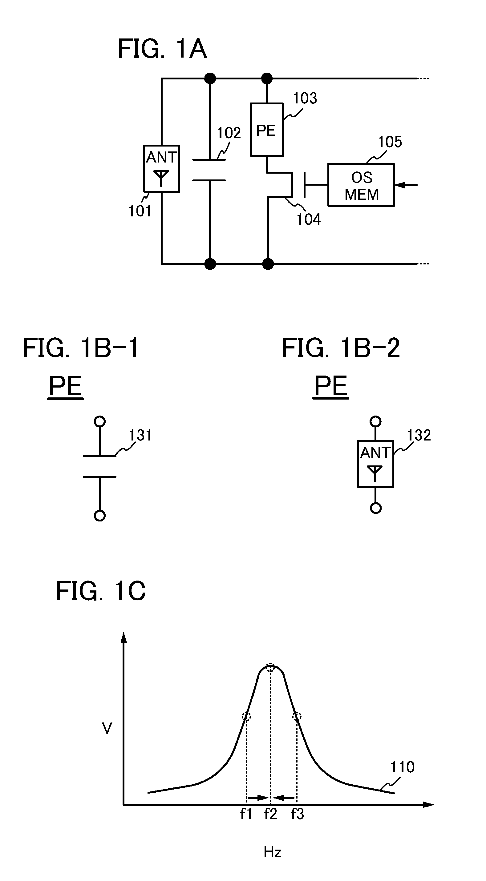
[0044]In this embodiment, an example of a semiconductor device in which the resonance frequency can be adjusted will be described.

[0045]An example of the semiconductor device in this embodiment will be described with reference to FIGS. 1A, 1B-1, 1B-2, and 1C.

[0046]The semiconductor device shown in FIG. 1A includes an antenna (also referred to as ANT) 101, a capacitor 102, a passive element (also referred to as PE) 103, a transistor 104, and a memory circuit (also referred to as OSMEM) 105.

[0047]Note that the transistor includes two terminals and a current control terminal for controlling current flowing between the two terminals by voltage applied. Note that without limitation to the transistor, in an element, terminals between which current flows and the current is controlled are also referred to as current terminals. Two current terminals are also referred to as a first current terminal and a second current terminal.

[0048]A field effect transistor can be used as the transistor, fo...

embodiment 2

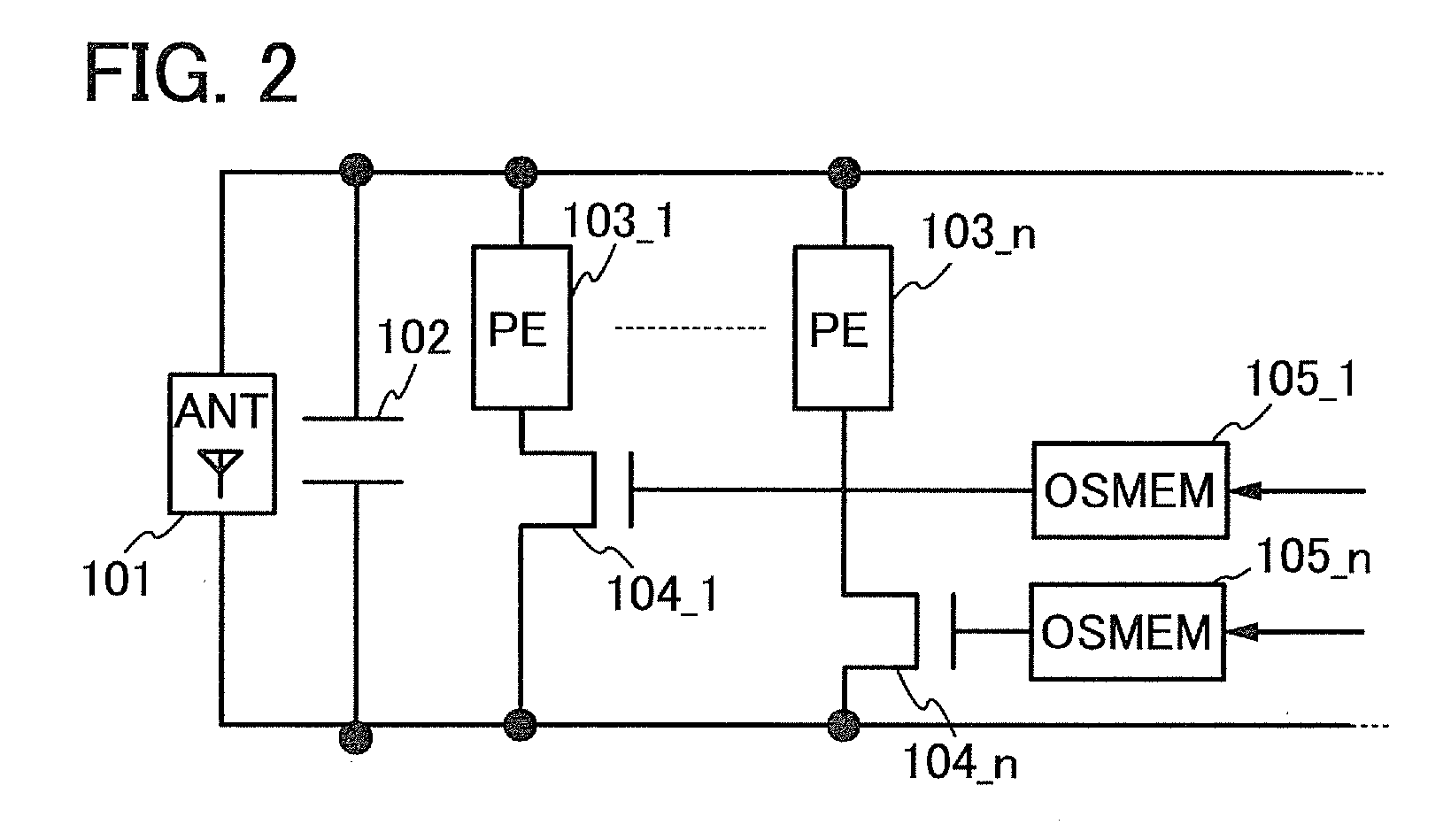
[0073]In this embodiment, an example of the semiconductor device described in Embodiment 1 will be described.

[0074]An example of a semiconductor device in this embodiment will be described with reference to FIG. 3. Note that in FIG. 3, the description of the semiconductor device shown in FIG. 1A is used as appropriate for components denoted by the same reference numerals as those in the semiconductor device shown in FIG. 1A.

[0075]The semiconductor device shown in FIG. 3 includes the antenna 101, the capacitor 102, the passive element 103, the transistor 104, and the memory circuit 105, similarly to the semiconductor device shown in FIG. 1A.

[0076]The antenna 101 functions as a coil.

[0077]The capacitor 102 is electrically connected to the antenna 101 in parallel.

[0078]The passive element 103 forms a resonance circuit when electrically connected to the antenna 101 and the capacitor 102 in parallel.

[0079]The transistor 104 has a function of controlling whether the passive element 103 is...

embodiment 3

[0094]In this embodiment, another example of the semiconductor device described in Embodiment 1 will be described.

[0095]Examples of memory circuits in this embodiment will be described with reference to FIGS. 4A and 4B. FIGS. 4A and 4B are diagrams for describing the memory circuits in this embodiment. Note that in FIGS. 4A and 4B, the description of the semiconductor device shown in FIG. 1A is used as appropriate for components denoted by the same reference numerals as those in the semiconductor device shown in FIG. 1A.

[0096]Semiconductor devices shown in FIGS. 4A and 4B each include the antenna 101, the capacitor 102, the passive element 103, the transistor 104, and the memory circuit 105 similarly to the semiconductor device shown in FIG. 1A.

[0097]The antenna 101 functions as a coil.

[0098]The capacitor 102 is electrically connected to the antenna 101 in parallel.

[0099]The passive element 103 forms a resonance circuit when electrically connected to the antenna 101 and the capacito...


PUM


Abstract

A semiconductor device includes an antenna functioning as a coil, a capacitor electrically connected to the antenna in parallel, a passive element forming a resonance circuit with the antenna and the capacitor by being electrically connected to the antenna and the capacitor in parallel, a first field effect transistor controlling whether the passive element is electrically connected to the antenna and the capacitor in parallel or not, and a memory circuit. The memory circuit includes a second field effect transistor which includes an oxide semiconductor layer where a channel is formed and in which a data signal is input to one of a source and a drain. The gate voltage of the first field effect transistor is set depending on the voltage of the other of the source and the drain of the second field effect transistor.

Description

BACKGROUND OF THE INVENTION[0001]1. Field of the Invention[0002]One embodiment of the present invention relates to a semiconductor device.[0003]2. Description of the Related Art[0004]In recent years, semiconductor devices have been developed which are capable of supplying (also referred to as feeding) power (also referred to as a power supply voltage) through wireless communication, and further capable of transmitting and receiving data (also referred to as data communication) through wireless communication. For example, if a feeding function through wireless communication can be added to a portable information terminal (e.g., a cellular phone) which is an example of the semiconductor devices, the portable information terminal does not need to be connected to an external power feeding portion and can be fed more easily, for example, in any environment.[0005]An individual identification technology utilizing a radio frequency identification (RFID) tag is known as an example of semicon...

Claims


Application Information

Patent Timeline
Patent Type & Authority Applications(United States)
IPC IPC(8): H01L27/06
CPCH01L21/8252H01L27/0605H01L27/0629H01L27/1225H01L23/66H01L2924/0002H01L27/1255H01L2924/00B42D25/305G06K19/077H04B5/02H01L23/5222H01L23/528H01L23/535H01L27/0733H01L29/41758H01L29/7869H03C2200/0029H03H7/1741H03J1/00H03J3/10H02J50/12
Inventor YONEDA, SEIICHI
Owner SEMICON ENERGY LAB CO LTD
Why Eureka
Try Eureka