

Method for fabricating novel semiconductor and optoelectronic devices
a technology of optoelectronic devices and semiconductors, applied in semiconductor devices, solid-state devices, transistors, etc., can solve the problems of less efficient mixing of red, blue and green colors to form white light, much more expensive than pcleds, and rgb-led is still much more expensive than a pcled solution
- Summary
- Abstract
- Description
- Claims
- Application Information
AI Technical Summary
Problems solved by technology
Method used
Image

Examples
Embodiment Construction
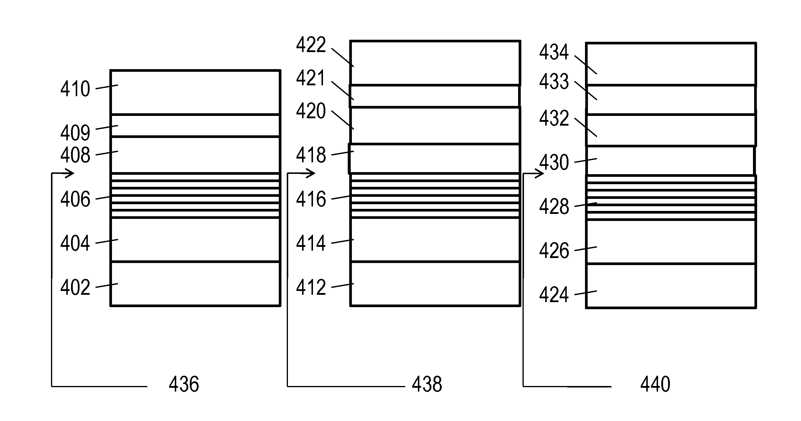
[0065]Embodiments of the present invention are now described with reference to FIGS. 1-30, it being appreciated that the figures illustrate the subject matter not to scale or to measure.
NuLED Technology:
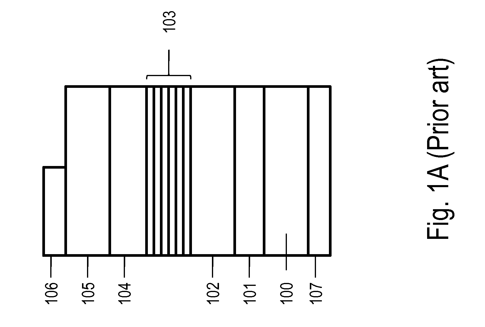
[0066]FIG. 1A illustrates a cross-section of prior art red LEDs. Red LEDs are typically constructed on a Gallium Arsenide substrate 100. Alternatively, Gallium Phosphide or some other material can be used for the substrate. Since Gallium Arsenide 100 is opaque, a Bragg Reflector 101 is added to ensure light moves in the upward direction. Red light is produced by a p-n junction with multiple quantum wells (MQW). A p-type confinement layer 104, a n-type confinement layer 102 and a multiple quantum well 103 form this part of the device. A current spreading region 105 ensures current flows throughout the whole device and not just close to the contacts. Indium Tin Oxide (ITO) could be used for the current spreading region 105. A top contact 106 and a bottom contact 107 are used for making...
PUM
 Abstract
Description
Claims
Application Information