Wafer-level electromagnetic interference shielding structure and manufacturing method thereof

a shielding structure and shielding technology, applied in the field of emi shielding structure, to achieve the effect of minimizing the emi shielding structur

Inactive Publication Date: 2012-09-27
UNIVERSAL SCIENTIFIC INDUSTRIAL (SHANGHAI) CO LTD +1
View PDF0 Cites 3 Cited by
  • Summary
  • Abstract
  • Description
  • Claims
  • Application Information

AI Technical Summary

Benefits of technology

[0008]Per aforementioned, the wafer-level EMI shielding structure provided by an embodiment of the present invention has the effect of miniaturizing EMI shielding structure. By utilizing wafer-level manufacturing method, and utilizing the first shielding layer and the second shielding layer respectively located at the surrounding surface of the wafer and the bottom of the wafer, the EMI shielding unit is formed, and thereby both the wafer and the exposed circuit unit both possess effect of EMI interference prevention.

Problems solved by technology

Manufacturing technologies related to EMI shielding structures uses substrate and electronic circuit components for various kinds of electrical coupling, so that the overall physical structure is large, or the final product becomes overly thick, which goes counter to the modern trend of thinner and smaller electronic products.

Method used


Image

  • Wafer-level electromagnetic interference shielding structure and manufacturing method thereof
  • Wafer-level electromagnetic interference shielding structure and manufacturing method thereof
  • Wafer-level electromagnetic interference shielding structure and manufacturing method thereof

Examples


Embodiment Construction

[0020]The aforementioned illustrations and following detailed descriptions are exemplary for the purpose of further explaining the scope of the present invention. Other objectives and advantages related to the present invention will be illustrated in the subsequent descriptions and appended drawings.

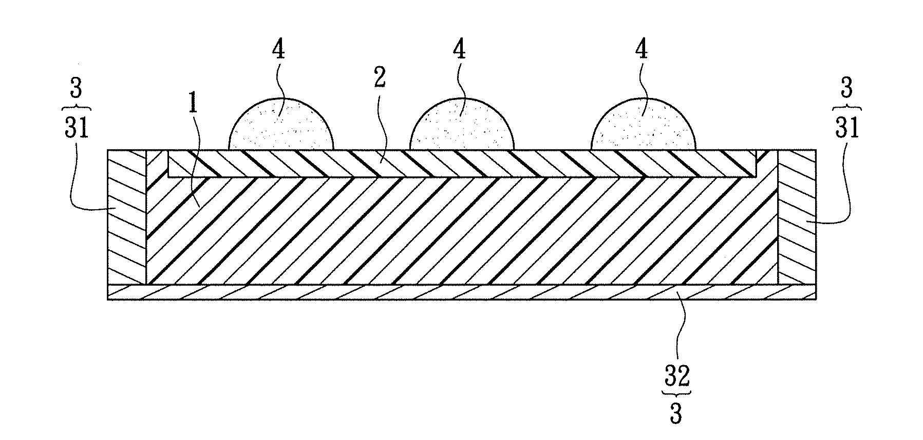
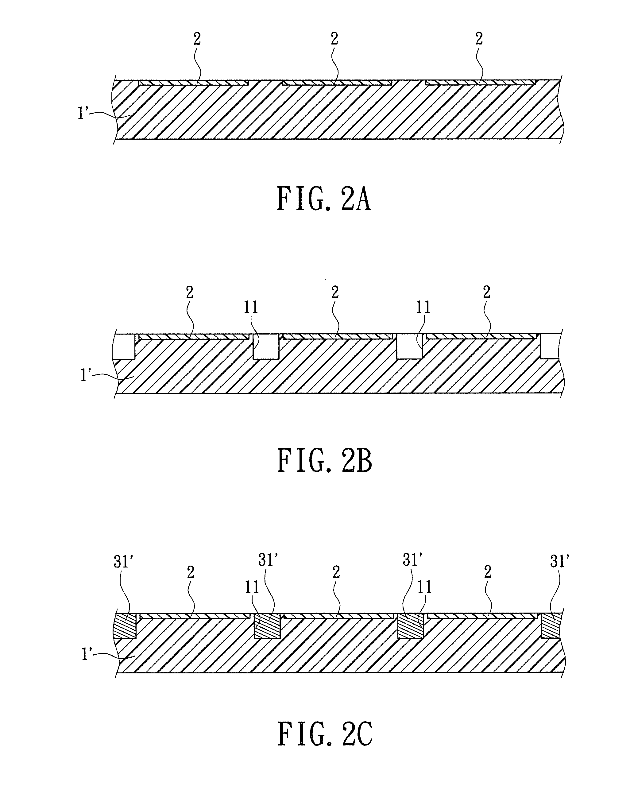
[0021]Reference FIG. 1, which shows a cross-sectional view of a wafer-level electromagnetic interference (EMI) shielding structure according to an embodiment of the present invention. The wafer-level EMI shielding structure according to an embodiment of the present invention includes: a wafer 1, an exposed circuit unit 2, and an EMI shielding unit 3.

[0022]The wafer 1 can be made from a silicon wafer substrate material. The top surface of the wafer 1 is disposed with the exposed circuit unit 2, and at least one conductor 4 is disposed on the exposed circuit unit 2. Also, the conductor 4 can be a solder ball or other conducting bump (such as metallic bump), so as to ensure possession of ex...


PUM

PropertyMeasurementUnit
EMI shieldingaaaaaaaaaa
conductingaaaaaaaaaa
physical structureaaaaaaaaaa

Abstract

A wafer-level electromagnetic interference (EMI) shielding structure, which includes: a wafer, an exposed circuit unit, and an EMI shielding unit. The exposed circuit unit is disposed on the top surface of the wafer. At least one conductor is disposed on the exposed circuit unit. The EMI shielding unit has a first EMI shielding layer set around the surrounding surface of the wafer, and a second EMI shielding layer coated to the bottom surface of the wafer. Based on the wafer-level manufacturing process of the instant disclosure, the EMI shielding structure is miniaturized, and each individual wafer is protected against the EMI effect.

Description

BACKGROUND OF THE INVENTION[0001]1. Field of the Invention[0002]The present invention relates to an electromagnetic interference (EMI) shielding structure; in particular, to a wafer-level EMI shielding structure and manufacturing method thereof.[0003]2. Description of Related Art[0004]The primary purpose of EMI shielding structure is to prevent the effect of electromagnetic interference from occurring between each electronic circuit components, and structural wise is primarily formed from combination of substrate unit, electronic circuit unit, metallic shielding unit, and electrical coupling unit. Electronic circuit components with EMI shielding structure can be widely applied to all kinds of everyday products, such as applications of notebook computers, mobile phones, e-book readers, electronic tablets, electronic gaming console, communication products, digital photo frames, mobile navigation systems, and digital televisions.[0005]Manufacturing technologies related to EMI shielding...

Claims


Application Information

Patent Timeline
Patent Type & Authority Applications(United States)
IPC IPC(8): H05K9/00H05K3/10
CPCH01L23/552H01L24/13H01L2224/131Y10T29/49155H01L2924/10253H01L23/3114H01L2924/014
Inventor WU, MING-CHE
Owner UNIVERSAL SCIENTIFIC INDUSTRIAL (SHANGHAI) CO LTD
Why Eureka
Try Eureka