Semiconductor manufacturing method for die bonding

a technology of die bonding and semiconductors, which is applied in the direction of machines/engines, semiconductor/solid-state device details, liquid fuel engines, etc., can solve the problems of difficult control of the supplying amount of paste, difficult to keep a high-precise discharge performance, and difficult to ensure low cost and efficient parts cleaning, etc., to reduce the manufacturing setup time of the gear, reduce the cost taken, and eliminate the effect of assembling adjustment tim

Inactive Publication Date: 2006-07-27
RENESAS TECH CORP
View PDF7 Cites 3 Cited by
  • Summary
  • Abstract
  • Description
  • Claims
  • Application Information

AI Technical Summary

Benefits of technology

[0092] A brief description will be given to the effects obtained by the representative aspects of the present invention disclosed in the present application.
[0093] The non-contact gear and the contact gear are processed so as to be concentric and integral, thereby being capable of reducing cost taken for the manufacture and assembly, such as the reduction in manufacturing setup time of the gear or elimination of assembling adjustment time. As a result, manufacturing cost can be reduced. Further, the gear pump has less number of components, so that reduction in cost and miniaturization can be achieved. According to this, the cost for the semiconductor manufacturing device to which the gear pump is incorporated can be reduced, and further, the mounting space of the gear pump can be decreased, thereby being capable of miniaturizing the semiconductor manufacturing device.

Problems solved by technology

An air pump of the pumps for supplying the adhesive has a problem that it is difficult to keep a high-precise discharge performance and to secure low cost and efficient parts cleaning.
Accordingly, there arises a problem that it is extremely difficult to perform a control of the supplying amount of the paste in a short period.

Method used


Image

  • Semiconductor manufacturing method for die bonding
  • Semiconductor manufacturing method for die bonding
  • Semiconductor manufacturing method for die bonding

Examples


embodiment

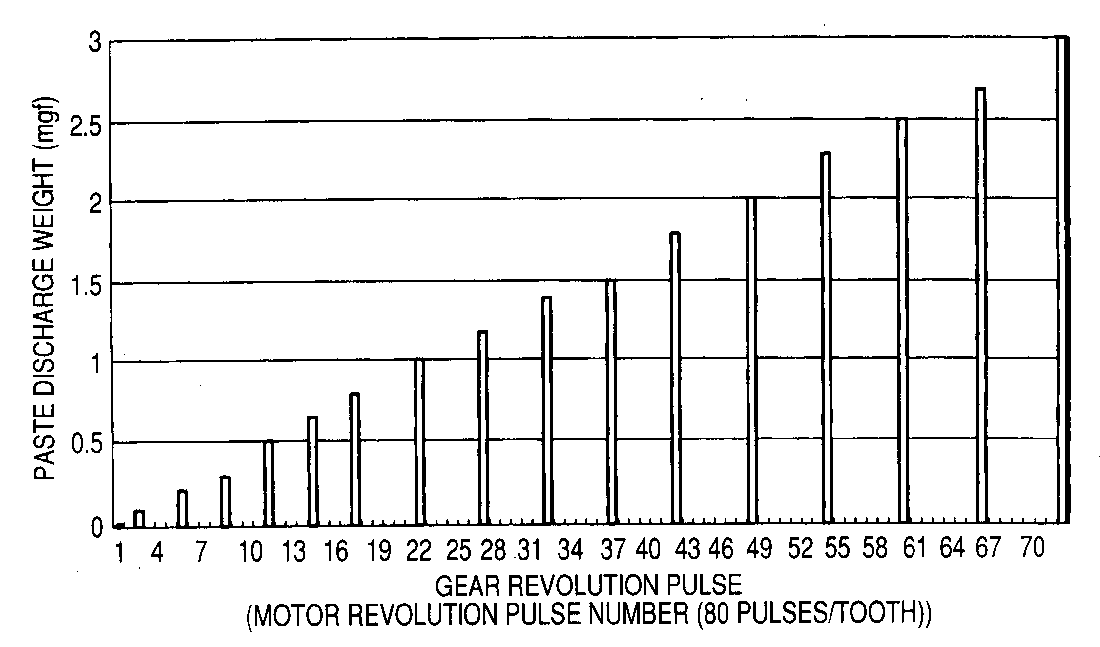
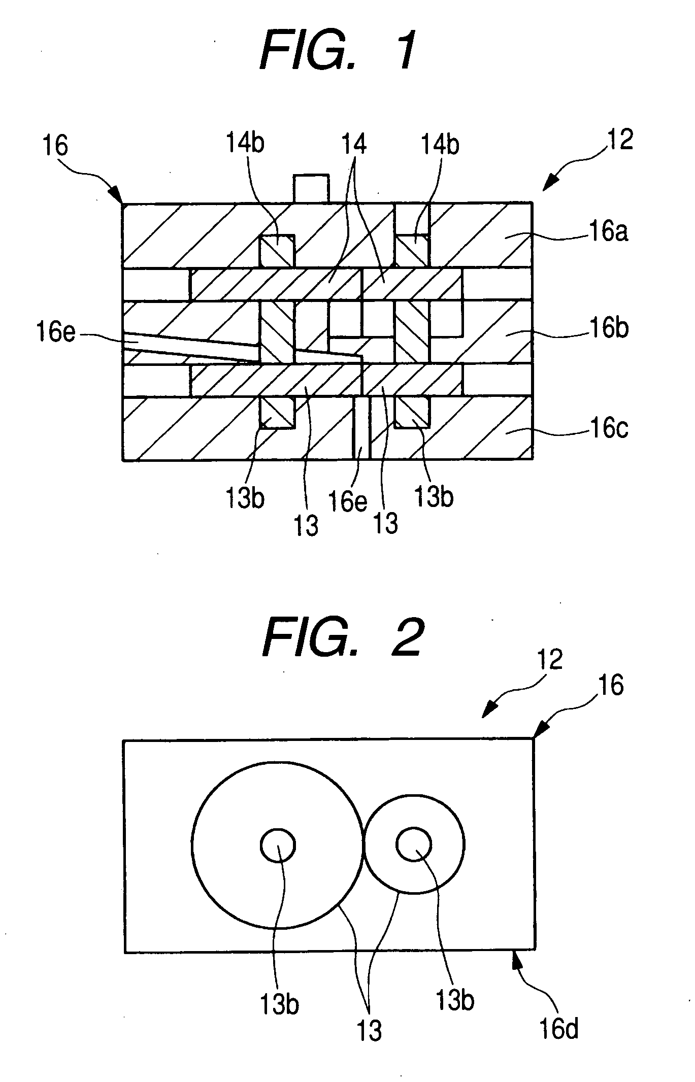
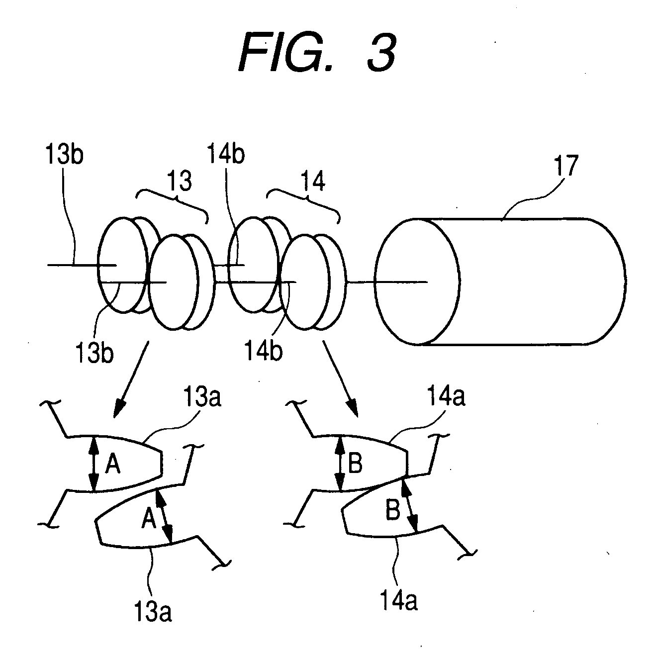
[0118]FIG. 1 is a sectional view showing one example of a structure of a gear pump used for assembling a semiconductor device according to the embodiment of the present invention; FIG. 2 is a back side view showing the structure of the gear pump shown in FIG. 1; FIG. 3 is a perspective view and partial enlarged view respectively showing a gear structure incorporated in the gear pump shown in FIG. 1 and a tooth profile; FIG. 4 is a sectional view showing one example of a structure of a pump system provided with the gear pump shown in FIG. 1; FIG. 5 is a sectional view showing one example of a structure of a semiconductor manufacturing device having incorporated therein the pump system shown in FIG. 4 and a state of an applied paste; FIG. 6 is a plan view showing one example of a state in which the paste shown in FIG. 5 is applied on a frame; FIG. 7 is a graph of a paste discharge amount showing one example of a pump performance of the pump system shown in FIG. 4; FIG. 8 and FIG. 9 ar...


PUM


Abstract

The present invention has a pump system having a gear pump to which a gear structure, having a pump gear and a driving gear concentrically and integrally formed with each other, is incorporated; a main control section for controlling this pump system; and a stage that can support a plate-like member such as a lead frame. In the gear pump, driving force is given to the driving gear to rotate the pump gear, whereby a paste is applied on the plate-like member. The use of the gear pump allows the reduction in cost for manufacturing and assembling the gears, thereby being capable of reducing manufacturing cost.

Description

CROSS-REFERENCE TO RELATED APPLICATION [0001] The present application claims priority from Japanese patent application No. 2005-018358 filed on Jan. 26, 2005, the content of which is hereby incorporated by reference into this application. BACKGROUND OF THE INVENTION [0002] This invention is related to a semiconductor manufacturing technique, and more particularly, to a technique effectively applicable to manufacture using a gear pump. [0003] A viscous fluid applying device has a discharge nozzle, nozzle rotating device, screw pump, screw rotating device and adhesive supplying device on a Z-axis slide that is moved in a direction parallel to the surface of a print wiring board by an XY direction moving robot. The discharge nozzle is concentrically provided at a pump housing, and the screw is rotatably provided in a screw chamber, wherein an adhesive is supplied by the adhesive supplying device. (e.g., see Patent Reference 1). [0004] In a pushing device for viscous fluid, a bottom cov...

Claims


Application Information

Patent Timeline
Patent Type & Authority Applications(United States)
IPC IPC(8): H01L21/302
CPCF04C2/084F04C13/002F04C2220/20F04C2220/28H01L21/561H01L21/565H01L23/3128H01L24/27H01L24/45H01L24/48H01L24/743H01L24/85H01L24/97H01L2224/45144H01L2224/48091H01L2224/48227H01L2224/48463H01L2224/73265H01L2224/743H01L2224/83192H01L2224/92H01L2224/97H01L2924/01004H01L2924/01005H01L2924/01014H01L2924/01079H01L2924/01082H01L2924/15311H01L2924/30105H01L2924/00014H01L2224/85H01L2224/83H01L2224/32225H01L2924/01006H01L2924/01033H01L24/29H01L24/83H01L2924/00H01L2224/92247H01L2924/00012H01L24/73H01L2924/181
Inventor OKAYAMA, MASAO
Owner RENESAS TECH CORP
Why Eureka
Try Eureka