Open hole-based diffractive light modulator

a diffractive light and open-hole technology, applied in the field of diffractive light modulators, can solve the problems of poor reliability in the control of light, light modulator described in the patent of bloom has a limitation in achieving miniaturization, light modulator has a limitation, etc., and achieve the effect of minimizing goods

Inactive Publication Date: 2006-04-13
SAMSUNG ELECTRO MECHANICS CO LTD
View PDF3 Cites 12 Cited by
  • Summary
  • Abstract
  • Description
  • Claims
  • Application Information

AI Technical Summary

Benefits of technology

[0018] Accordingly, the present invention has been made keeping in mind the above problems occurring in the prior art, and an object of the present invention is to provide a diffractive light modulator in which one pixel is formed using as few as one ribbon element, thereby miniaturizing goods.

Problems solved by technology

However, the light modulator by Bloom adopts an electrostatic method to control the position of a micromirror, which is disadvantageous in that operation voltage is relatively high (usually 30 V or so) and the relationship between the applied voltage and displacement is not linear, thus resulting in poor reliability in the control of light.
However, the light modulator described in the patent of Bloom has a limitation in achieving miniaturization.
That is, the light modulator has a limitation in that the widths of the elements thereof cannot be formed to be below 3 μm and the interval between elements cannot be formed to be below 0.5 μm.
Furthermore, a minimum of two elements is required to constitute a diffraction pixel, thus having a limitation in the miniaturization of a device.

Method used


Image

  • Open hole-based diffractive light modulator
  • Open hole-based diffractive light modulator
  • Open hole-based diffractive light modulator

Examples


first embodiment

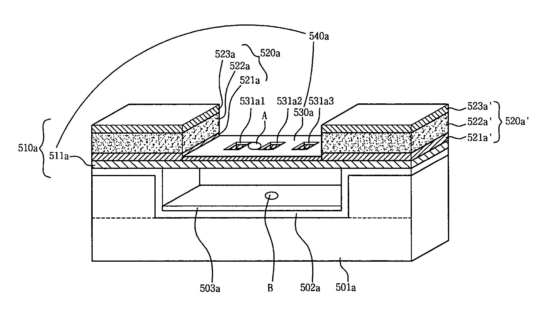
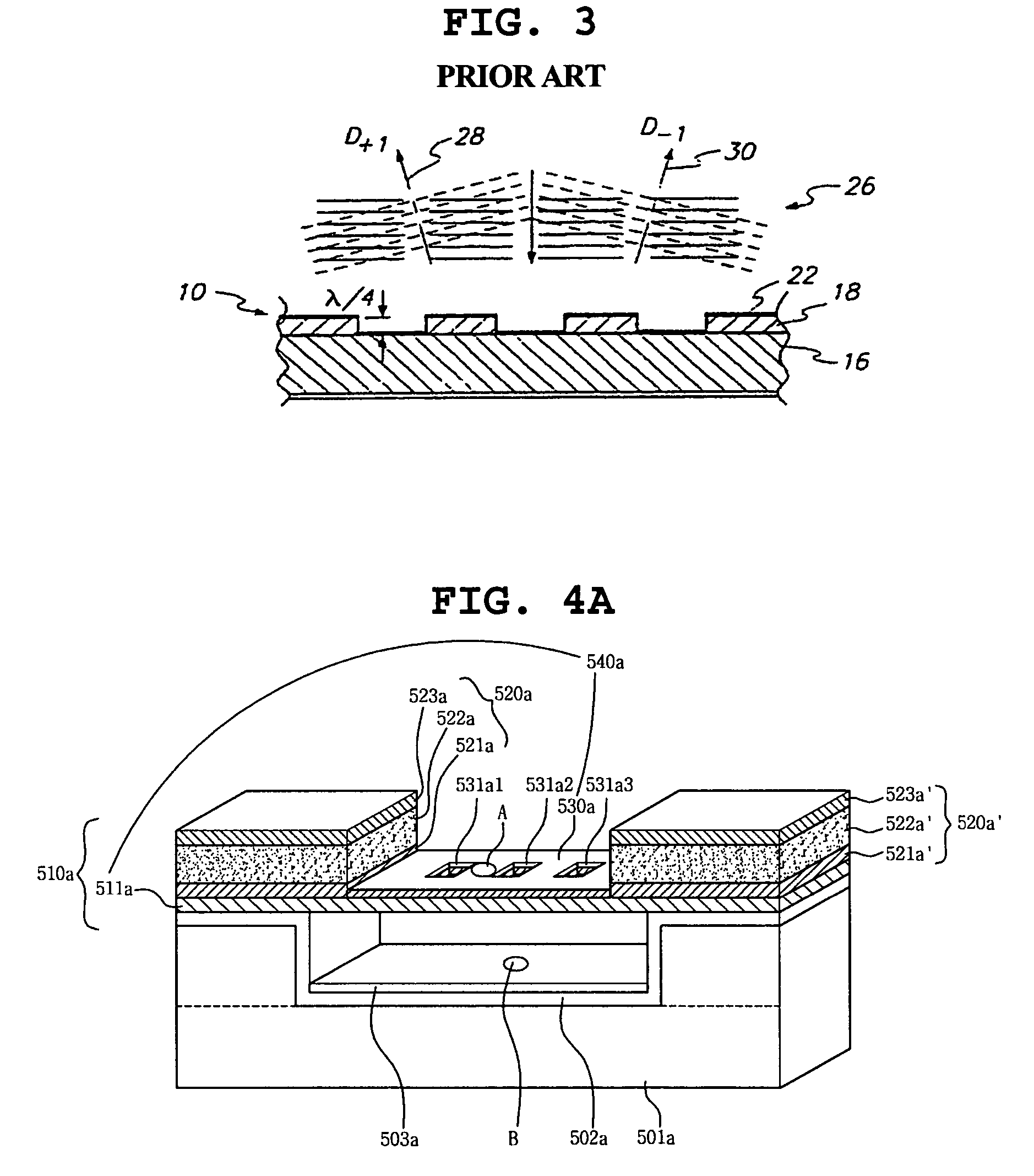
[0045]FIG. 4a is a perspective view of an open hole-based diffractive light modulator, according to the present invention.

[0046] Referring to the drawing, the open hole-based diffractive light modulator according to the first embodiment of the present invention includes a silicon substrate 501a, an insulating layer 502a, a micromirror 503a, and an element 510a. Although the insulating layer and the micromirror are illustrated as constructed in separate layers in this embodiment, the insulating layer can be implemented to function as the lower micromirror if it has light-reflective characteristics. Furthermore, herein, the insulating layer 502a is shown as formed on a surface of the base member 501a, but the insulating layer is not essential, thus the reflective part 503a may be formed without forming the insulating layer 502a.

[0047] The silicon substrate 501a includes a recess for providing a space for the element 510a, the insulating layer 502a is formed on the silicon substrate 5...

second embodiment

[0063]FIG. 4b is a perspective view of an open hole-based diffractive light modulator, which is partially broken away, according to the present invention.

[0064] Referring to the drawing, the open hole-based diffractive light modulator according to the second embodiment of the present invention comprises a base member 501b, a lower reflective part 503b and an element 510b.

[0065] Unlike the first embodiment, the lower reflective part 503b includes a plurality of lower reflective patterns 503b1-503b3, and the plurality of lower reflective patterns 503b1-503b3 is provided on the surface of an insulating layer 502a at intervals so that they correspond in position to open holes 531b1-531b3 of an upper micromirror 530b. The other constructions are the same as those of FIG. 4a.

third embodiment

[0066]FIG. 4c is a perspective view of an open hole-based diffractive light modulator, which is partially broken away, according to the present invention.

[0067] Referring to the drawing, the open hole-based diffractive light modulator according to the third embodiment of the present invention comprises a base member 501c which includes a SIMOX SOI (separation by implanted oxygen silicon-on-insulator) substrate (hereinafter, referred to as “silicon-on-insulator substrate”), a lower reflective part 503c, and an element 510c.

[0068] The third embodiment of the present invention is different from the first embodiment of FIG. 4a in that the silicon-on-insulator substrate, rather than a silicon substrate, is used as the base member 501c. Its fabrication is well known, thus a detailed description of it is omitted herein.

[0069] The base member 501c of the silicon-on-insulator used in the present invention comprises a silicon substrate 501c1, a silicon oxide insulating layer 501c2 which is ...


PUM


Abstract

This invention relates to a diffractive light modulator. Particularly, the invention relates to an open-hole based diffractive light modulator. In the modulator, a lower reflective part is provided on a base member and open holes are formed through an upper micromirror raised from the base member so that one pixel is formed using one element having the ribbon-shaped upper micromirror.

Description

BACKGROUND OF THE INVENTION [0001] 1. Field of the Invention [0002] The present invention relates, in general, to a diffractive light modulator and, more particularly, to an open-hole based diffractive light modulator, in which a lower reflective part is provided on a base member and open holes are formed through an upper micromirror raised from the base member so that one pixel is formed using one element having the upper micromirror. [0003] 2. Description of the Related Art [0004] Generally, an optical signal processing technology has advantages in that a great amount of data is quickly processed in a parallel manner unlike a conventional digital information processing technology in which it is impossible to process a great amount of data in real time. Studies have been conducted on the design and production of a binary phase filter, an optical logic gate, a light amplifier, an image processing technique, an optical device, and a light modulator using a spatial light modulation th...

Claims


Application Information

Patent Timeline
Patent Type & Authority Applications(United States)
IPC IPC(8): G02B26/00
CPCG02B26/0808
Inventor YUN, SANG KYEONG
Owner SAMSUNG ELECTRO MECHANICS CO LTD
Why Eureka
Try Eureka