

Semiconductor integrated circuit device
- Summary
- Abstract
- Description
- Claims
- Application Information
AI Technical Summary
Benefits of technology
Problems solved by technology
Method used
Image

Examples
embodiments
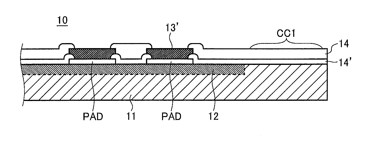
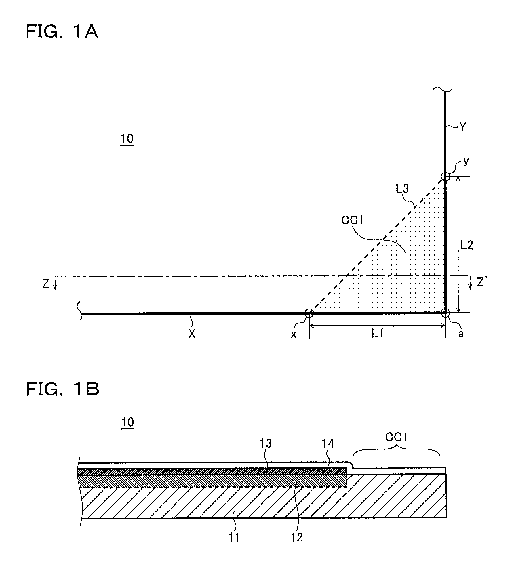
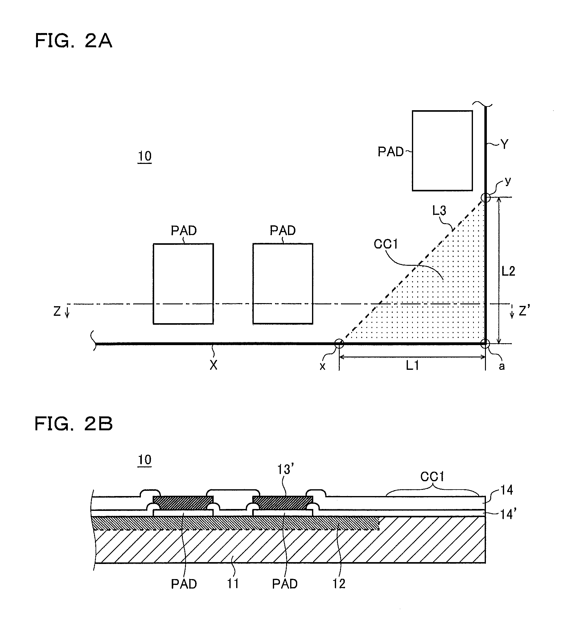
[0023]FIG. 1A is a top view and FIG. 1B is a sectional view taken along line Z-Z′ in FIG. 1A, both showing a semiconductor integrated circuit device according to a first embodiment of the present invention.
[0024]As shown in FIG. 1A, the semiconductor integrated circuit device 10 of this embodiment is a semiconductor chip cut apart along prescribed dicing lines, and dividing it apart gives it four corners and four edges each connecting two adjoining corners. FIG. 1A shows, of all these corners and edges, only one corner “a” and two edges X and Y extending from it in mutually perpendicular directions.
[0025]As shown in FIG. 1B, in the semiconductor integrated circuit device 10 of this embodiment, an element forming region (impurity diffusion region) 12 is formed on a semiconductor substrate 11 cut out in a rectangular shape, and further on top a metal wiring layer 13 and then a passivation layer 14 are formed. The semiconductor substrate 11 is cut out so that one side thereof is at lea...
PUM
 Abstract
Description
Claims
Application Information