Display device

a display device and display screen technology, applied in the field of display devices, can solve the problems of reducing affecting the recognition of touch locations, and affecting the resolution of captured images, so as to reduce the resolution. the effect of the decreas

Inactive Publication Date: 2012-09-27
SHARP KK
View PDF3 Cites 14 Cited by
  • Summary
  • Abstract
  • Description
  • Claims
  • Application Information

AI Technical Summary

Benefits of technology

[0006]The display device of the present invention will reduce the decrease

Problems solved by technology

This may reduce resolution.
As a result, resolution of a captured image

Method used


Image

  • Display device
  • Display device
  • Display device

Examples


first embodiment

[0035

[0036]Referring first to FIGS. 1 and 2, the configuration of a TFT substrate 100 included in a photosensor-incorporating liquid crystal display device LCD (see FIGS. 4B and 4C) as a display device according to a first embodiment of the present invention will be described.

[0037][Configuration of TFT Substrate]

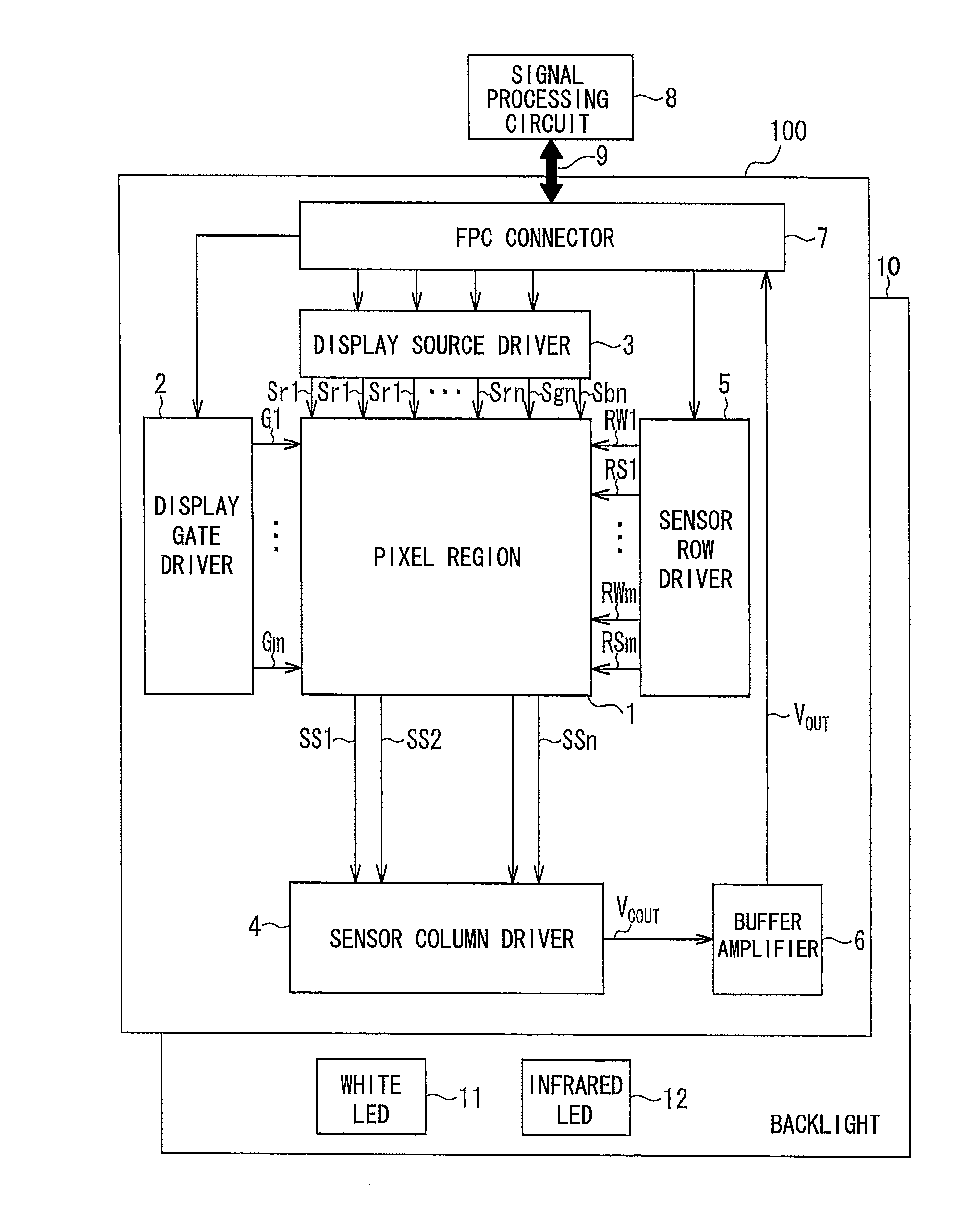
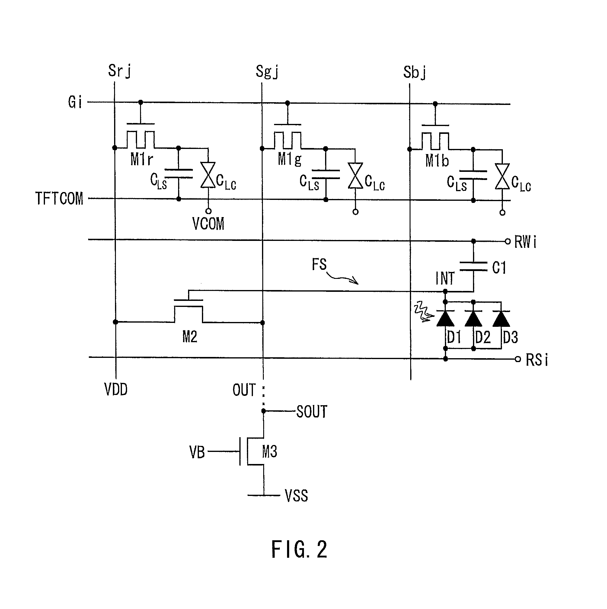
[0038]FIG. 1 is a block diagram that schematically shows a TFT substrate 100 included in a liquid crystal display device LCD. As shown in FIG. 1, the TFT substrate 100 at least includes, on a glass substrate, a pixel region 1, a display gate driver 2, a display source driver 3, a sensor column driver 4, a sensor row driver 5, a buffer amplifier 6, and an FPC connector 7. Further, a signal processing circuit 8 for processing an image signal received by a plurality of photosensor assemblies FS (see FIG. 2), described later, provided in the pixel region 1 is connected to the TFT substrate 100 via the FPC connector 7 and an FPC 9.

[0039]The pixel region 1 is a region where a pix...

second embodiment

[0102

[0103]FIG. 9 is a cross sectional view of a liquid crystal display device as a display device according to a second embodiment, illustrating a set of light receivers and a set of sensor apertures. FIG. 9 shows an arrangement of one photosensor assembly, i.e. one photosensor unit. In the implementation shown in FIG. 9, the photosensor assembly includes three light receivers (in this implementation, photodiodes D1, D2 and D3 as examples) arranged in one direction and three sensor apertures formed above. The portions other than those shown in FIG. 9 may be the same as those shown in FIGS. 1 to 4 of the first embodiment.

[0104]As shown in FIG. 9, the present embodiment provides a metal layer 27 between a black matrix 22 and light receivers D1, D2 and D3. One aperture 18 is formed in the black matrix 22 for one photosensor unit. Sensor apertures 28a, 28b and 28c are provided in the metal layer 27. Opening is controlled by the sensor apertures 28a, 28b and 28c. That is, sensor apertur...

third embodiment

[0125

[0126]FIG. 11 is a cross sectional view of a liquid crystal display device as a display device according to a third embodiment, illustrating a set of light receivers and a set of sensor apertures. FIG. 11 shows the arrangement of one photosensor assembly, i.e. one photosensor unit. In the implementation shown in FIG. 11, the photosensor assembly includes three light receivers (in this present implementation, photodiodes D1, D2 and D3 as examples) arranged in one direction and one sensor aperture 18 formed above. The portions other than those shown in FIG. 11 may be the same as those shown in FIGS. 1 to 4 of the first embodiment.

[0127]As shown in FIG. 11, in the present embodiment, a metal layer 27 is provided between the black matrix 22 and the light receivers D1, D2 and D3. One aperture 18 is formed in the black matrix 22 for one photosensor unit. One sensor aperture 28 is provided in the metal layer 27. Opening is controlled by this aperture. That is, a sensor aperture 28 hav...


PUM


Abstract

Decrease in resolution is minimized even in a photosensor including a plurality of receivers. In a photosensor-equipped display device including a plurality of photosensor assemblies in a display region that displays an image, each of the photosensor assemblies includes: a plurality of sensor apertures (18a-18c) that allow light to enter the display device through a display surface for the image in the display region; and a plurality of light receivers (D1-D3) provided below the respective sensor apertures (18a-18c) for receiving light entering the display device through the sensor apertures (18a-18c) and converting the light into an electric signal, and the plurality of sensor apertures (18a-18c) and the plurality of light receivers (D1-D3) are arranged in at least one direction, and at least one (18a, 18c) of the plurality of sensor apertures (18a-18c) that is located outward is displaced inward relative to at least one of the light receivers (D1-D3) that is located below that at least one sensor aperture.

Description

TECHNICAL FIELD[0001]The present invention relates to a display device having a photosensor such as a photodiode or a phototransistor.BACKGROUND ART[0002]Photosensor-equipped display devices have been proposed that include, in a pixel, a light detection element such as a photodiode that is capable of measuring the brightness of external light or capturing an image of an object located close to the display, for example. In such a photosensor- equipped display device, for example, at least one light detection element is provided as a light receiver for each pixel. In such a photosensor- equipped display device where one or more light detection elements are provided for each pixel, providing two or more light detection elements as one sensor unit has been proposed in order to ensure sufficient electric signals to allow an object located close to the display to be detected (see, for example, JP2001-320547A, JP2004-45875A, JP2008-97171A, and JP2008-262204A).DISCLOSURE OF THE INVENTION[00...

Claims


Application Information

Patent Timeline
IPC IPC(8): G09G5/00
CPCG06F3/0412G02F2001/13312G02F1/13318G06F3/042G02F1/13312
Inventor YUKI, RYUZOUSUKURA, NARU
Owner SHARP KK
Why Eureka
Try Eureka