Light emitting device and method for manufacturing the same

a technology of light emitting device and manufacturing method, which is applied in the direction of semiconductor/solid-state device manufacturing, semiconductor devices, electrical devices, etc., can solve the problems of uneven light emission, low light extraction efficiency, and difficult to obtain uniform white light, and achieve uniform light emission and light extraction efficiency. satisfactory

Active Publication Date: 2012-10-04
NICHIA CORP
View PDF3 Cites 40 Cited by
  • Summary
  • Abstract
  • Description
  • Claims
  • Application Information

AI Technical Summary

Benefits of technology

[0010]Thus, an object of the present invention is to provide a light emitting device that has satisfactory light extraction efficiency and enables uniform light emission, and a method for manufacturing the same.
[0021]According to the present invention, it is possible to provide a light emitting device that has satisfactory light extraction efficiency and enables uniform light emission, and a method for manufacturing the same. According to the light emitting device of the present invention, it is also possible to provide a light emitting device having light distribution characteristics close to that of the point light source.

Problems solved by technology

However, in this way, it is hard to obtain uniform white light because a difference occurs in the quantity of blue light absorbed by the phosphor according to difference in a length of an optical path of the blue light from the light emitting element.
Further, light emission from the phosphor layer provided on the wiring pattern may induce uneven light emission.
Further, in JP-A-2003-69086, the light emitted from the light emitting element is absorbed by the wiring pattern around the light emitting element, which lowers light extraction efficiency.
It is difficult to completely fill the space between the light emitting element and the substrate with the phosphor particles, and thus a density of the phosphor particles tends to be lower than that of the other areas.
As a result, light from the light emitting element may leak therefrom.

Method used


Image

  • Light emitting device and method for manufacturing the same
  • Light emitting device and method for manufacturing the same
  • Light emitting device and method for manufacturing the same

Examples


first embodiment

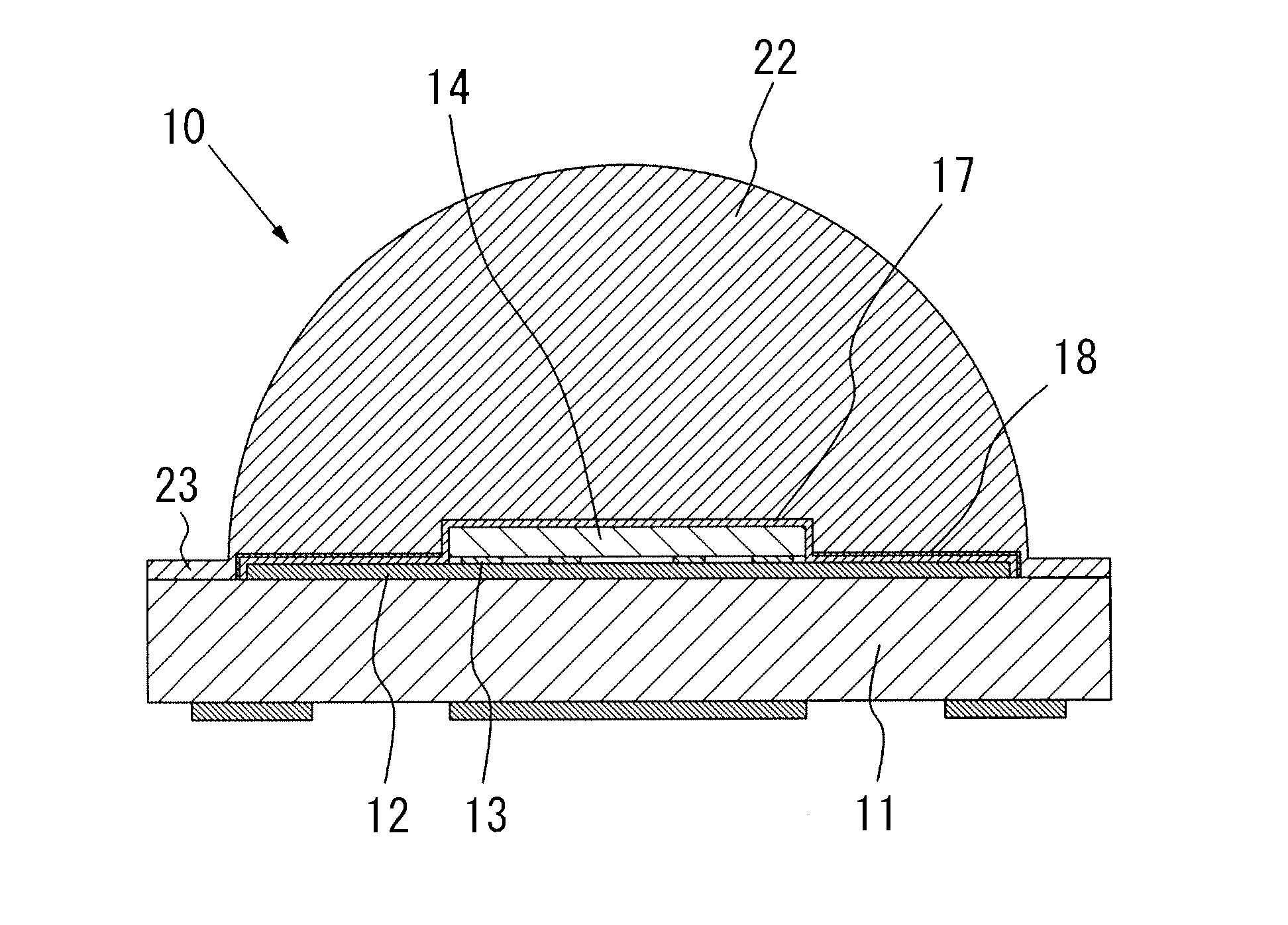
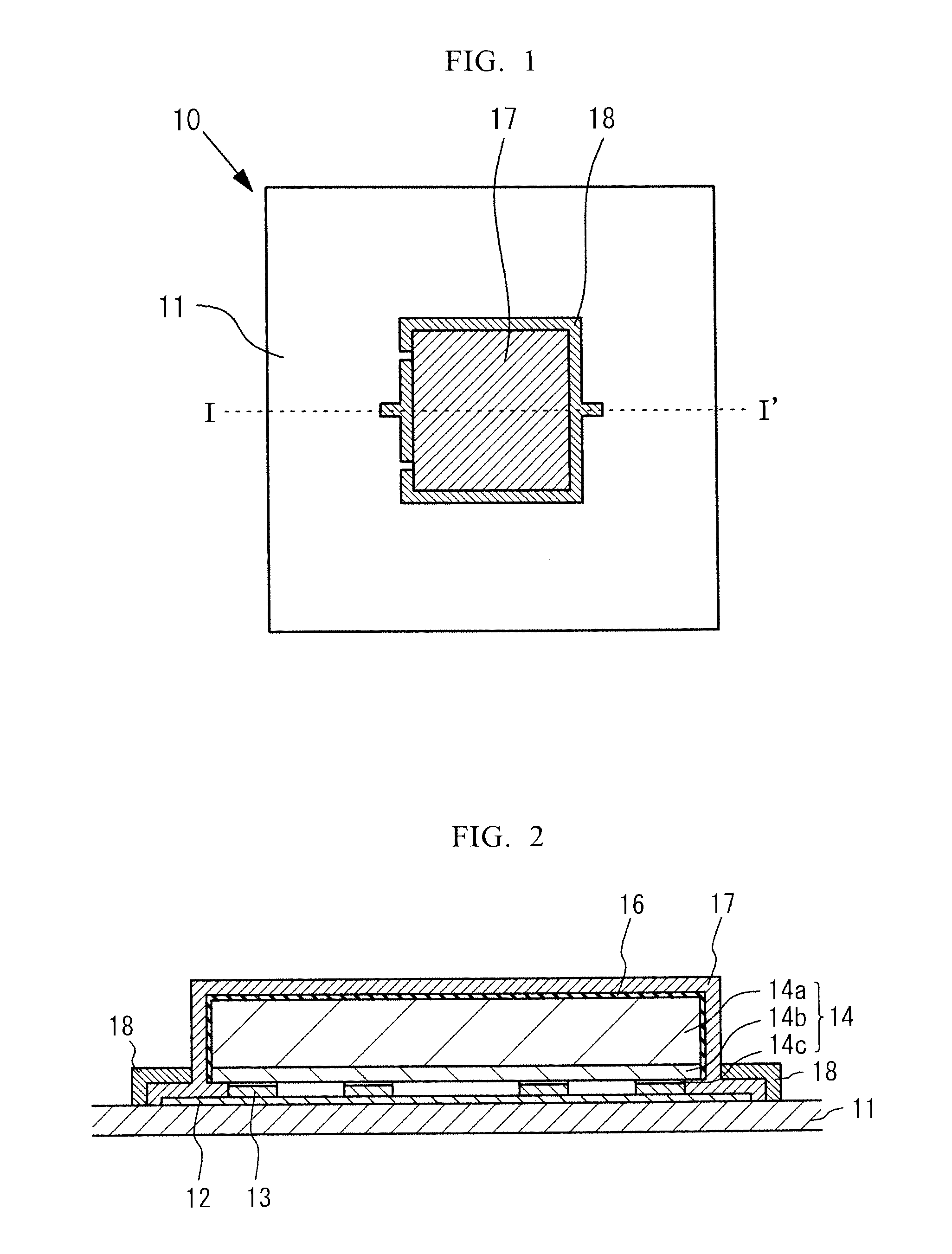
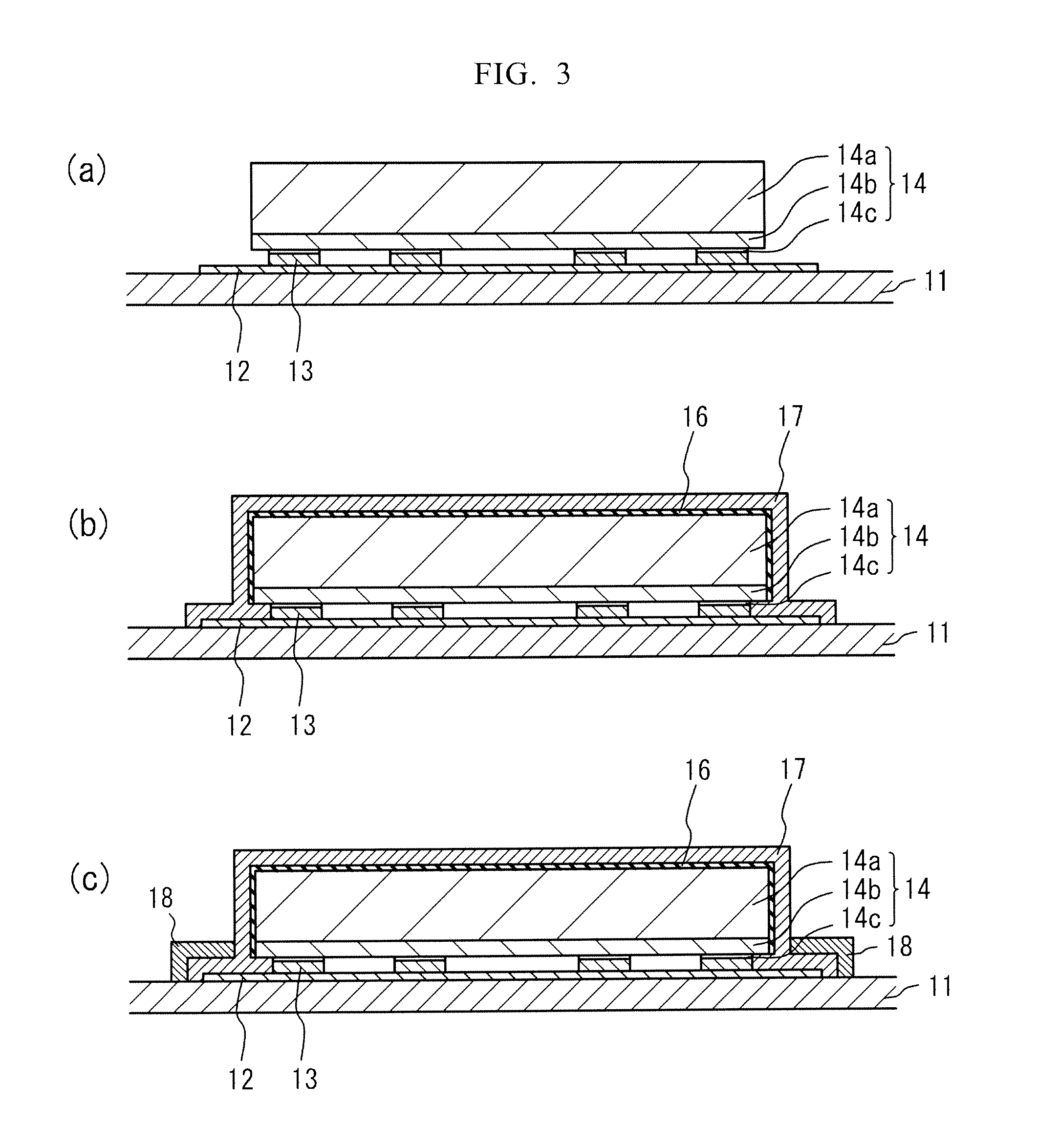
[0033]FIG. 1 is a schematic plan view showing an example of a light emitting device according to a first embodiment of the present invention. FIG. 2 is a schematic cross-sectional view of the light emitting device taken along line I-I′ of FIG. 1.

[0034]A light emitting device 10 according to the present embodiment includes a substrate 11 having a conductive portion 12, a light emitting element 14, a phosphor layer 17, and a reflection layer 18.

[0035]The substrate 11 is shaped into a substantially plate-like shape and has the conductive portion 12 on a part thereof. The light emitting element 14 includes a semiconductor layer 14b including a luminescent layer formed on one main surface of a transparent substrate 14a having a pair of opposing main surfaces. The light emitting element 14 further has a positive electrode and a negative electrode (hereinafter referred to as “electrodes 14c”) formed on a surface of the semiconductor layer 14b. In the light emitting device of the first embo...

second embodiment

[0075]FIG. 4 is a schematic plan view showing an example of a light emitting device according to the second embodiment of the present invention. Descriptions of configurations identical to those of the light emitting device according to the first embodiment are omitted.

[0076]In the light emitting device 10 according to the present embodiment, a protection element 19 such as a Zener diode is positioned on the substrate 11. The conductive portion 12 is formed on the substrate 11, except for an area where the protection element 19 is positioned, into a substantially circular shape centering the area in which the light emitting element 14 is positioned. The phosphor layer 17 and the reflection layer 18 are formed so as to cover almost the entire exposed area of the conductive portion 12. The reflection layer 18 may be formed so as to cover the protection element 19. Whereby, the light extraction efficiency of the light emitting device of the present embodiment in the upper surface of th...

third embodiment

[0078]A light emitting device according to the third embodiment is described below. Descriptions of configurations identical to those of the light emitting device according to the first embodiment are omitted. FIG. 5 is a schematic plan view showing an example of the light emitting device according to the third embodiment of the present invention. FIG. 6 is a schematic sectional view of the light emitting device taken along line III-III′ of FIG. 5.

[0079]In the light emitting device 10 according to the present embodiment, the conductive portion 12 is formed on the substrate 11, except for the area in which the protection element 19 is positioned, into a substantially circular shape centering the area in which the light emitting element 14 is positioned. The conductive portion 12 has grove shaped openings 12a along the outer edge of the light emitting element around the area in which the light emitting element 14 is positioned and the substrate 11 is partially exposed at the openings ...


PUM


Abstract

A light emitting device includes a substrate having a conductive portion; a light emitting element having one or more electrodes on a lower surface side thereof, the electrodes being positioned on the conductive portion of the substrate; a phosphor layer disposed on a surface of the light emitting element and on a peripheral surface area of the conductive portion next to the light emitting element; and a reflection layer covering a part of the phosphor layer disposed on the peripheral surface area of the conductive portion.

Description

BACKGROUND OF THE INVENTION[0001]1. Field of the Invention[0002]The present invention relates to a light emitting device including a light emitting element and a phosphor layer, and a method for manufacturing the same.[0003]2. Description of the Related Art[0004]Generally, a light emitting device using a light emitting element such as a light emitting diode (LED) has electronic parts such as a light emitting element and a protection element, a substrate on which the elements are positioned, and a transparent resin for protecting the light emitting element, the protection element and the like.[0005]A technique is known in which, for the purpose of causing the light emitting device to emit white light, a concave portion is provided on the substrate, a light emitting element for emitting blue light is positioned in the concave portion, and a transparent resin including a phosphor is provided so that the phosphor covers the light emitting element in the concave portion. In the light emi...

Claims


Application Information

Patent Timeline
Patent Type & Authority Applications(United States)
IPC IPC(8): H01L33/60H01L33/30
CPCH01L33/44H01L33/505H01L2224/13H01L2933/0041H01L33/60H01L33/46H01L33/50
Inventor BEPPU, SUGURUNOICHI, TAKUYA
Owner NICHIA CORP
Why Eureka
Try Eureka