
Light emitting nitride semiconductor device and method of fabricating the same

A technology for nitride semiconductors and light-emitting devices, which is applied in the manufacture of semiconductor/solid-state devices, semiconductor devices, and electric solid-state devices, etc., can solve the problems of alignment of interconnect patterns 122 and solder joints 125, reduction of yield, etc.

Active Publication Date: 2005-10-12
XIAMEN SANAN OPTOELECTRONICS CO LTD
View PDF3 Cites 7 Cited by
  • Summary
  • Abstract
  • Description
  • Claims
  • Application Information

AI Technical Summary

Problems solved by technology

However, since the chip 123 and the layer 124 are mounted on the substrate through the pads 125, it is difficult to align the interconnection pattern 122 with the pads 125, resulting in reduced yield.

Method used


Image

  • Light emitting nitride semiconductor device and method of fabricating the same
  • Light emitting nitride semiconductor device and method of fabricating the same
  • Light emitting nitride semiconductor device and method of fabricating the same

Examples


no. 1 example

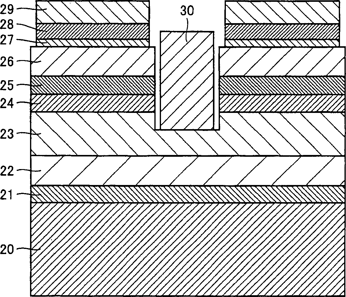
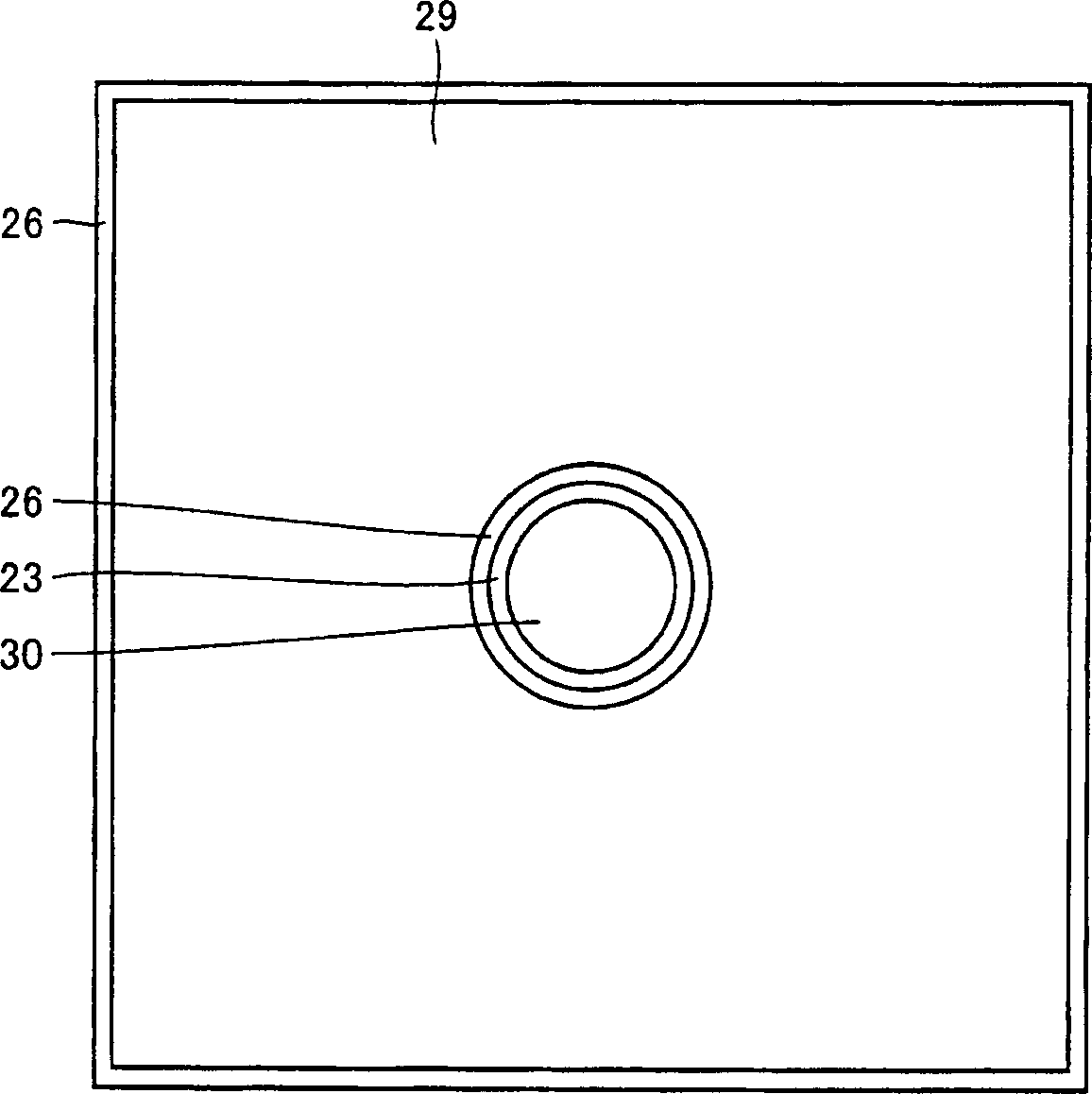
[0056] figure 2 A cross-sectional structure of the present light emitting device formed of a GaN-based compound semiconductor on a sapphire substrate is shown. image 3 is a plan view viewed from its top surface.

[0057] On the substrate 20 made of sapphire, a GaN buffer layer 21 is deposited. An undoped 1 [mu]m GaN layer 22 is deposited thereon. A 4 μm thick nGaN layer 23 of silicon-doped GaN is deposited thereon. These layers provide an electrode layer having a first conductivity. Furthermore, on the nGaN layer 23, a GaN barrier layer and a light emitting multiple quantum well layer 24 composed of an InGaN well layer are deposited in layers to provide a light emitting layer. A p-type cladding layer 25 made of p-type AlGaN is deposited on the light emitting layer 24 as an electrode layer having the second conductivity. A p-type contact layer 26 made of p-type GaN is deposited on the p-type cladding layer 25 .

[0058] On the p-type contact layer 26, the second electro...

no. 2 example

[0069] Figure 5 is a schematic cross-sectional view of the light-emitting nitride semiconductor device structure, Figure 6 is a plan view viewed from its top surface. exist Figure 5 Among them, the present light-emitting device has a light-emitting device structure formed of a GaN-based compound semiconductor deposited on a sapphire substrate.

[0070] This embodiment is similar to the first embodiment until the first electrode is formed. Next, the back surface of the sapphire substrate 20 was polished so as to have a conical hole whose tip was about 50 [mu]m from the surface of the supporting electrode. In addition, this conical hole is formed at the same pitch as the electrode formation pattern, and the tip of the hole is located at the center of the electrode pattern.

[0071] After that, the back surface of sapphire substrate 20 is polished again so that its thickest part has a thickness of about 100 [mu]m. Thereafter, the back surface of the substrate was provided...

no. 3 example

[0074] Figure 8 is a schematic cross-sectional view of the light-emitting nitride semiconductor device structure, Figure 9 is a plan view viewed from its bottom. exist Figure 8 Among them, the present light-emitting device has a light-emitting device structure formed of a GaN-based compound semiconductor deposited on a GaN substrate.

[0075] This embodiment is similar to the first embodiment until the bonding electrode layer 29 is formed. Next, the back surface of GaN substrate 40 was polished so as to have a conical hole whose tip was about 50 [mu]m from the surface of the supporting electrode. In addition, this conical hole is formed at a pitch equal to the size of the chip, and the tip of the hole is located at the center of the chip.

[0076] After that, the back surface of GaN substrate 40 is polished again so that its thickest part has a thickness of about 100 μm. Thereafter, an n-type electrode 32 composed of 20 nm thick Ti and 200 nm thick Al provided by vapor...


PUM


Abstract

There is provided a light emitting nitride semiconductor device including a substrate, a semiconductor layer of a first conductivity overlying the substrate, a light emitting layer overlying the semiconductor layer of the first conductivity, a semiconductor layer of a second conductivity overlying the light emitting layer, and a second electrode overlying at least the semiconductor layer of the second conductivity, wherein the second electrode has a high reflectance for a main light emission wavelength and the light emitting device allows light to be extracted mainly at a side surface thereof.

Description

technical field [0001] The present invention relates to the use of nitride compound semiconductors (In x Al y Ga 1-x-y N, where 0≤X, 0≤Y, X+Y<1) is a light emitting nitride semiconductor device. Background technique [0002] Figure 11 The structure of a conventional light emitting nitride semiconductor device described in Japanese Patent Laying-Open (Japanese Patent Laying-Open) No. 08-274372 is shown in . In this figure, this conventional light emitting device has a sapphire substrate 101 on which a 500 Å thick Al 0.1 Ga 0.83 In 0.07 N buffer layer 102. On the buffer layer 102, a silicon-doped GaN is formed + layer 103, its thickness is about 2.0 μm, and its electron density is 2×10 18 / cm 3 . In addition to providing the part of the electrode 201, the n + Layer 103 is sequentially deposited: doped with silicon (Al x2 Ga 1-x2 ) y2 In 1-y2 N composed of n with high carrier concentration + layer 104, its thickness is about 2.0 μm, and its electron density ...

Claims


Application Information

Patent Timeline
Patent Type & Authority Applications(China)
IPC IPC(8): H01L21/283H01L31/18H01L33/06H01L33/32H01L33/40
CPCH01L33/20H01L33/382H01L33/405H01L2224/48091H01L2224/32245H01L2224/73265H01L2224/48247H01L2224/48257H01L2924/10158H01L2924/181H01L2224/73204H01L2224/16225H01L2224/32225H01L2924/00014H01L2924/00012H01L2924/00
Inventor 笔田麻佑子
Owner XIAMEN SANAN OPTOELECTRONICS CO LTD
Learn More