Light emitting device and method for manufacturing the same

a technology of light emitting device and manufacturing method, which is applied in the direction of semiconductor/solid-state device manufacturing, semiconductor devices, electrical devices, etc., can solve the problems of uneven light emission, low light extraction efficiency, and difficult to obtain uniform white light, and achieve uniform light emission and light extraction efficiency. satisfactory

Active Publication Date: 2014-09-16
NICHIA CORP
View PDF14 Cites 1 Cited by
  • Summary
  • Abstract
  • Description
  • Claims
  • Application Information

AI Technical Summary

Benefits of technology

[0010]Thus, an object of the present invention is to provide a light emitting device that has satisfactory light extraction efficiency and enables uniform light emission, and a method for manufacturing the same.
[0021]According to the present invention, it is possible to provide a light emitting device that has satisfactory light extraction efficiency and enables uniform light emission, and a method for manufacturing the same. According to the light emitting device of the present invention, it is also possible to provide a light emitting device having light distribution characteristics close to that of the point light source.

Problems solved by technology

However, in this way, it is hard to obtain uniform white light because a difference occurs in the quantity of blue light absorbed by the phosphor according to difference in a length of an optical path of the blue light from the light emitting element.
Further, light emission from the phosphor layer provided on the wiring pattern may induce uneven light emission.
Further, in JP-A-2003-69086, the light emitted from the light emitting element is absorbed by the wiring pattern around the light emitting element, which lowers light extraction efficiency.
It is difficult to completely fill the space between the light emitting element and the substrate with the phosphor particles, and thus a density of the phosphor particles tends to be lower than that of the other areas.
As a result, light from the light emitting element may leak therefrom.

Method used


Image

  • Light emitting device and method for manufacturing the same
  • Light emitting device and method for manufacturing the same
  • Light emitting device and method for manufacturing the same

Examples


example 1

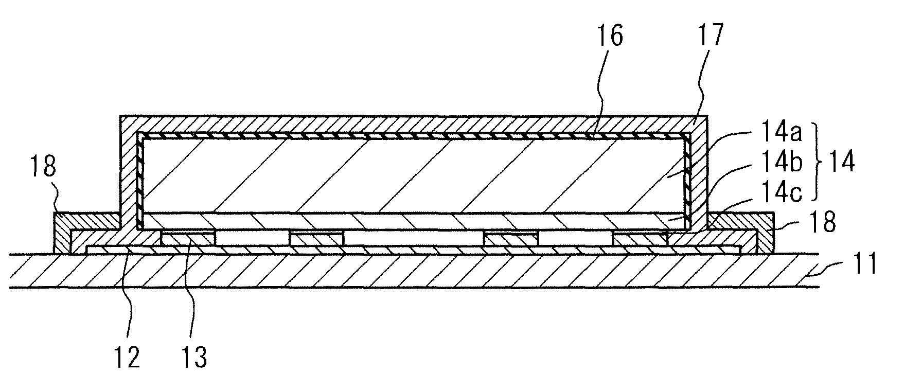
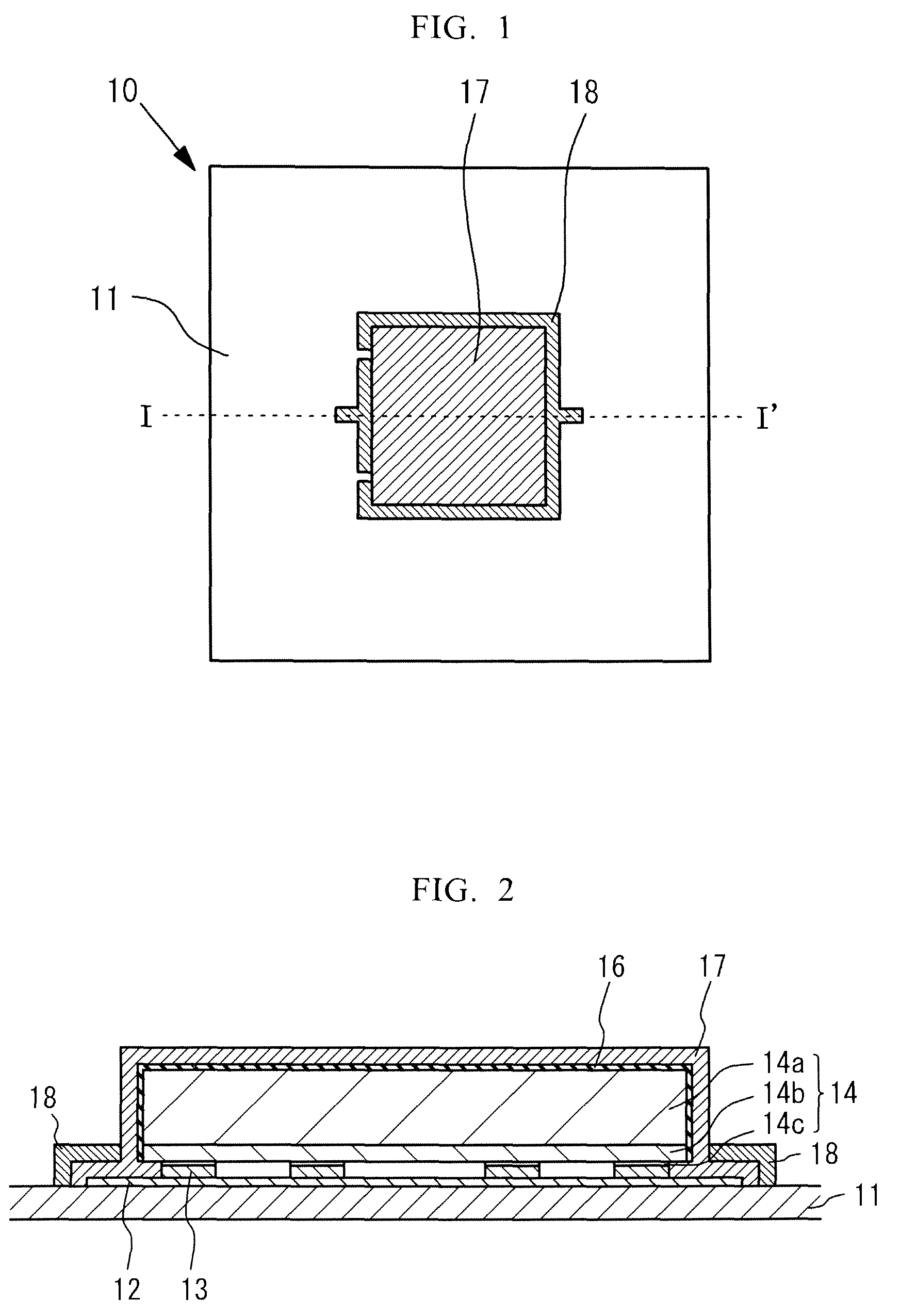
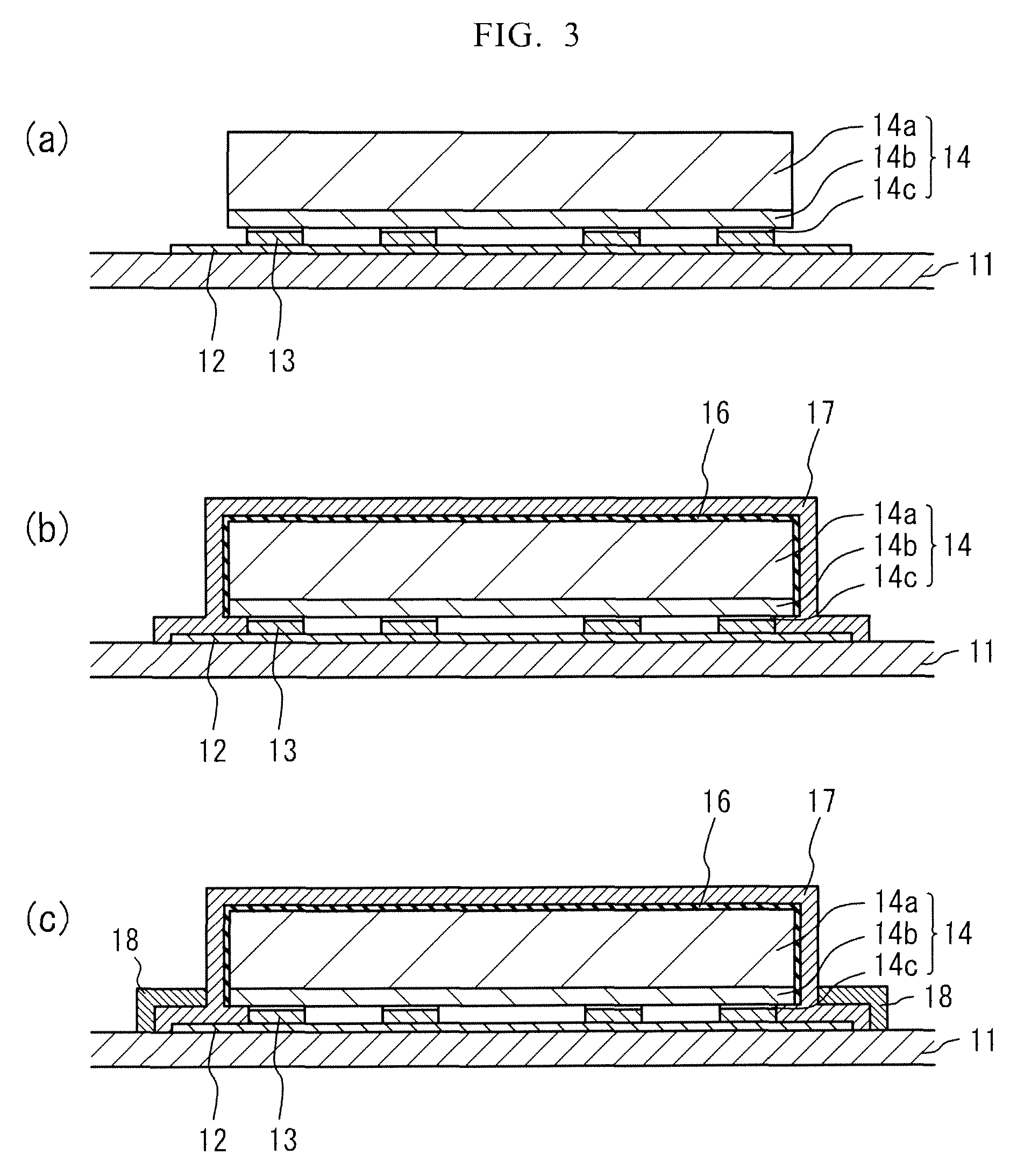
[0088]FIG. 9 is a schematic sectional view showing a light emitting device according to Example 1. The light emitting device includes the substrate 11 including the conductive portion 12, the bonding members 13, the light emitting element 14, the phosphor layer 17, and the reflection layer 18.

[0089]Alumina ceramics are used for forming the substrate 11 and Au is used for forming the conductive portion 12. The conductive portion 12 is partially embedded in the substrate 11. The conductive portion 12 functions as a terminal for electrically connecting the light emitting element 14 with the external power supply because the conductive portion 12 is exposed on a rear surface of the substrate 11.

[0090]The light emitting element 14 is connected to the conductive portion 12 by using bumps made of Au as the bonding members 13. The light emitting element 14 includes the substrate 14a made of sapphire having the insulating property and the semiconductor layer 14b formed on the substrate 14a. ...

example 2

[0094]FIG. 1 is a schematic sectional view showing the light emitting device according to Example 2. Example 2 differs from Example 1 in that Al is used for forming the covering layer 16, the covering layer 16 is reformed so as to have the insulating property after forming the phosphor layer 17, and TiO2 (having an average particle diameter of 0.3 μm) is used for forming the reflection layer 18. In the present Example, before forming the reflection layer 18, the covering layer 16 is oxidized to reform the covering layer 16 so as to have the insulating property by, for example, a method in which the covering layer 16 is heated under the water-vapor atmosphere. Accordingly, the reflection layer is not formed on the phosphor layer 17 formed on the light emitting element 14 through the covering layer 16 but the reflection layer 18 is formed only on the phosphor layer 17 formed on the conductive portion 12.

[0095]In the present Example, it is also possible to obtain a light emitting devic...

example 3

[0096]Example 3 differs from Example 1 in that Sn—Ag—Cu is used as the bonding members 13 and Mg is used for forming the covering layer 16. The phosphor layer 17 has an average particle diameter of the phosphor particles of 5 μm and is formed by the electrostatic coating method. BaSO4 (having an average particle diameter of 0.5 μm) is used for forming the reflection layer 18. The other points are identical to those of Example 1.

[0097]In the present Example, it is also possible to obtain a light emitting device that causes less uneven light emission and also has improved light extraction efficiency.


PUM


Abstract

A light emitting device includes a substrate having a conductive portion; a light emitting element having one or more electrodes on a lower surface side thereof, the electrodes being positioned on the conductive portion of the substrate; a phosphor layer disposed on a surface of the light emitting element and on a peripheral surface area of the conductive portion next to the light emitting element; and a reflection layer covering a part of the phosphor layer disposed on the peripheral surface area of the conductive portion.

Description

BACKGROUND OF THE INVENTION[0001]1. Field of the Invention[0002]The present invention relates to a light emitting device including a light emitting element and a phosphor layer, and a method for manufacturing the same.[0003]2. Description of the Related Art[0004]Generally, a light emitting device using a light emitting element such as a light emitting diode (LED) has electronic parts such as a light emitting element and a protection element, a substrate on which the elements are positioned, and a transparent resin for protecting the light emitting element, the protection element and the like.[0005]A technique is known in which, for the purpose of causing the light emitting device to emit white light, a concave portion is provided on the substrate, a light emitting element for emitting blue light is positioned in the concave portion, and a transparent resin including a phosphor is provided so that the phosphor covers the light emitting element in the concave portion. In the light emi...

Claims


Application Information

Patent Timeline
Patent Type & Authority Patents(United States)
IPC IPC(8): H01L33/44H01L33/50H01L33/60
CPCH01L33/505H01L33/60H01L33/44H01L2933/0041H01L2224/13H01L2924/0002H01L33/46H01L33/50
Inventor BEPPU, SUGURUNOICHI, TAKUYA
Owner NICHIA CORP
Why Eureka
Try Eureka