Double-sided light emitting field emission device and method of manufacturing the same

a technology of light-emitting field and emission device, which is applied in the manufacture of electric discharge tube/lamp, luminescent coating application, discharge tube luminescnet screen, etc., can solve the problems of limited application, reduced service life of carbon nanotube, and inability to utilize field emission device, etc., to reduce the field emission arcing effect, increase the overall illumination, and prolong the service life

Active Publication Date: 2012-10-04
NATIONAL CHUNG CHENG UNIV
View PDF0 Cites 27 Cited by
  • Summary
  • Abstract
  • Description
  • Claims
  • Application Information

AI Technical Summary

Benefits of technology

[0009]A one objective of the present invention is to provide a double-sided light-emitting field emission device and method of manufacturing the same, which combines phosphor and field emission source to form a two-electrode structure, without the need to differentiate them into anode or cathode, then AC voltage driving is used in achieving double-sided light emitting for raising the overall illumination.
[0010]Another objective of the present invention is to provide a double-sided light-emitting field emission device and method of manufacturing the same, such that the driving voltage required for the double-sided light-emitting field emission device thus produced is an AC voltage, so the field emission sources can be alternated depending on frequency rather than conducting continuous emission, hereby protecting the carbon nanotube field emission source, and prolonging its service life.
[00...

Problems solved by technology

In addition, due to its spontaneous light-emitting characteristics, the field emission device can not only be utilized as field emission display, but it can also be widely used as light-emitting device in backlight module or illumination light.
However, regardless of the type of electrodes, their common characteristics are that, they are all single-sided light emitting field emission light source, and thus having limited applicatio...

Method used


Image

  • Double-sided light emitting field emission device and method of manufacturing the same
  • Double-sided light emitting field emission device and method of manufacturing the same
  • Double-sided light emitting field emission device and method of manufacturing the same

Examples


Embodiment Construction

[0023]The purpose, construction, features, functions and advantages of the present invention can be appreciated and understood more thoroughly through the following detailed description with reference to the attached drawings.

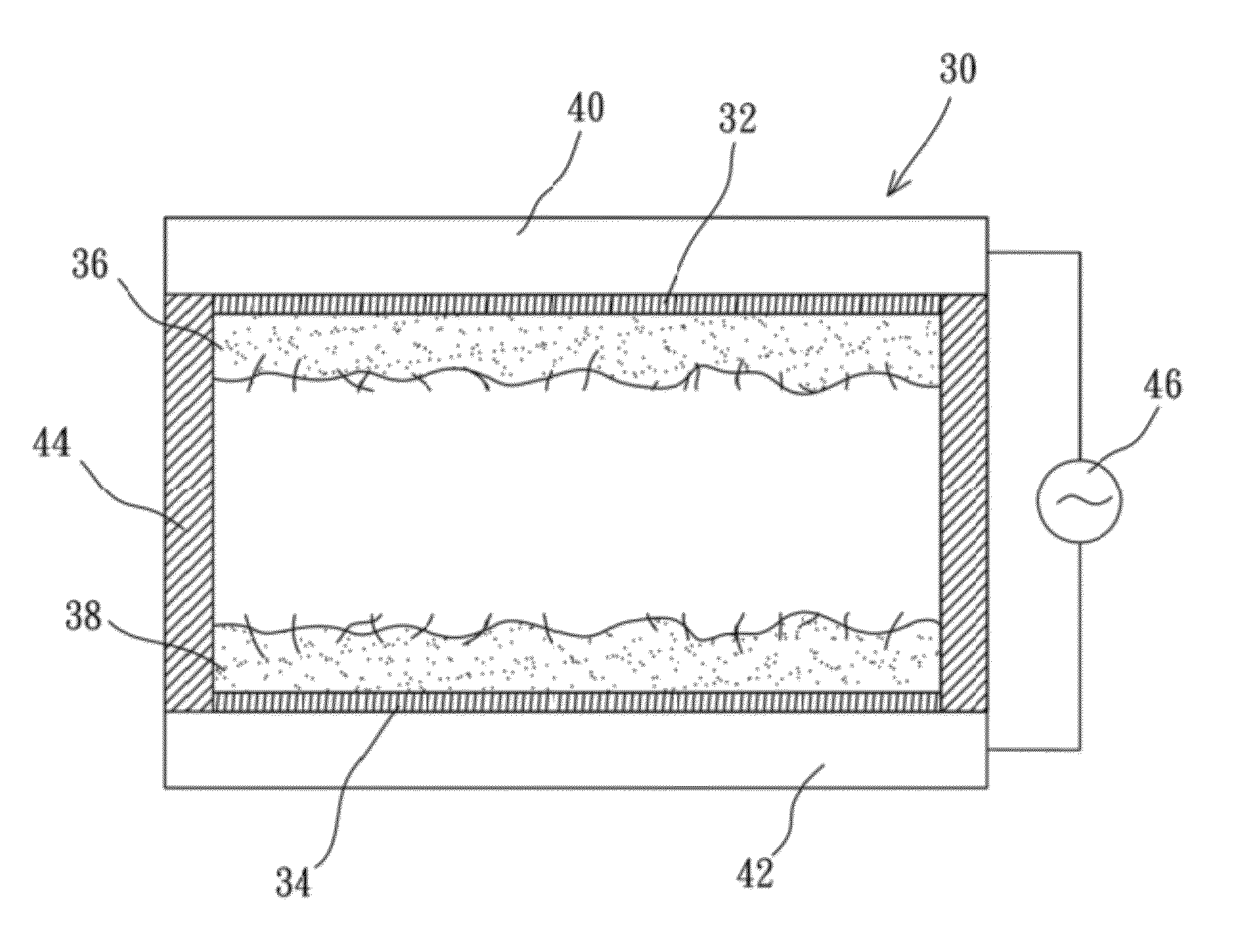
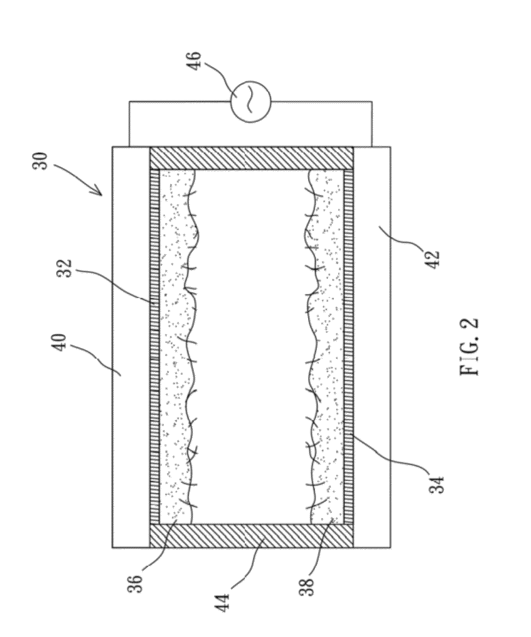
[0024]The present invention provides an innovative double-sided light-emitting field emission device and method of manufacturing the same, wherein, phosphor and field emission source are mixed at certain ratio to produce field emission devices of cathode / anode substrates. Due to the alternating nature of the positive and negative polarities of AC power source, the substrates of the field emission device may play the role of cathode or anode alternatively to form a two-electrode structure without having to distinguish them being anode or cathode. Therefore, it can emit lights alternatively by means of AC voltage driving in achieving double-sided light emitting.

[0025]Refer to FIG. 2 for a schematic diagram of the double-sided light-emitting field emission device ...


PUM


Abstract

A double-sided light-emitting field emission device and method of manufacturing same, said device comprising at least two transparent conductive layers, mixed field emission layers, and transparent package device. Wherein, the mixed field emission layer of field emission source and phosphor are utilized directly to serve as anode and cathode alternatively, such that on applying an AC power supply, roles of anode and cathode are changed alternatively along with frequency, hereby forming double-sided light-emitting structure. Therefore, the applications of said double-sided light-emitting field emission device are pretty wide, and having advantages of protecting field emission source, activating field emission source, reducing field emission arcing effect, having conductive phosphor, and raising illumination.

Description

BACKGROUND OF THE INVENTION[0001]1. Field of the Invention[0002]The present invention relates to a field emission device, and in particular to a double-sided light-emitting field emission device and method of manufacturing the same.[0003]2. The Prior Arts[0004]The Field Emission Display Technology incorporates and makes use of the technology of carbon nanotube, so that it is able to achieve great breakthrough and developments in various applications. In addition, due to its spontaneous light-emitting characteristics, the field emission device can not only be utilized as field emission display, but it can also be widely used as light-emitting device in backlight module or illumination light.[0005]In general, the basic structure of field emission device is composed of a phosphor plate serving as an anode, and a carbon nanotube serving as a cathode. As shown in FIG. 1, the field emission device includes two glass substrates, an upper substrate 12 and a lower substrate 10, and a spacer ...

Claims


Application Information

Patent Timeline
IPC IPC(8): H01J19/24B82Y40/00H01J9/22B82Y99/00H01J9/26
CPCH01J1/304H01J63/06H01J9/22H01J29/04H01J29/18H01J31/127H01J2201/30469H01J2201/30496H01J2329/0407H01J2329/0455H01J2329/0473H01J2329/18H01J63/02H01J63/04H01J9/025
Inventor LI, YUAN-YAOYOUH, MENG-JEYTSENG, CHUN-LUNGWU, HUNG-CHIHLIN, WANG-HUAJUAN, YEN-MINGCHIU, SHENG-CHENG
Owner NATIONAL CHUNG CHENG UNIV
Why Eureka
Try Eureka