Nonvolatile semiconductor memory device

a non-volatile, semiconductor technology, applied in static storage, digital storage, instruments, etc., can solve the problems of data reading operation failure, memory cell data change,

Active Publication Date: 2012-10-11
KIOXIA CORP
View PDF1 Cites 26 Cited by
  • Summary
  • Abstract
  • Description
  • Claims
  • Application Information

AI Technical Summary

Problems solved by technology

As the miniaturization of NAND type flash memories progresses, interference between adjoining cells and influence due to elapse of time after data writing increase, which might change the memory cell data.
If deterioration of data retention occurs, a data reading operation may fail.

Method used


Image

  • Nonvolatile semiconductor memory device
  • Nonvolatile semiconductor memory device
  • Nonvolatile semiconductor memory device

Examples


first embodiment

[0040][Configuration]

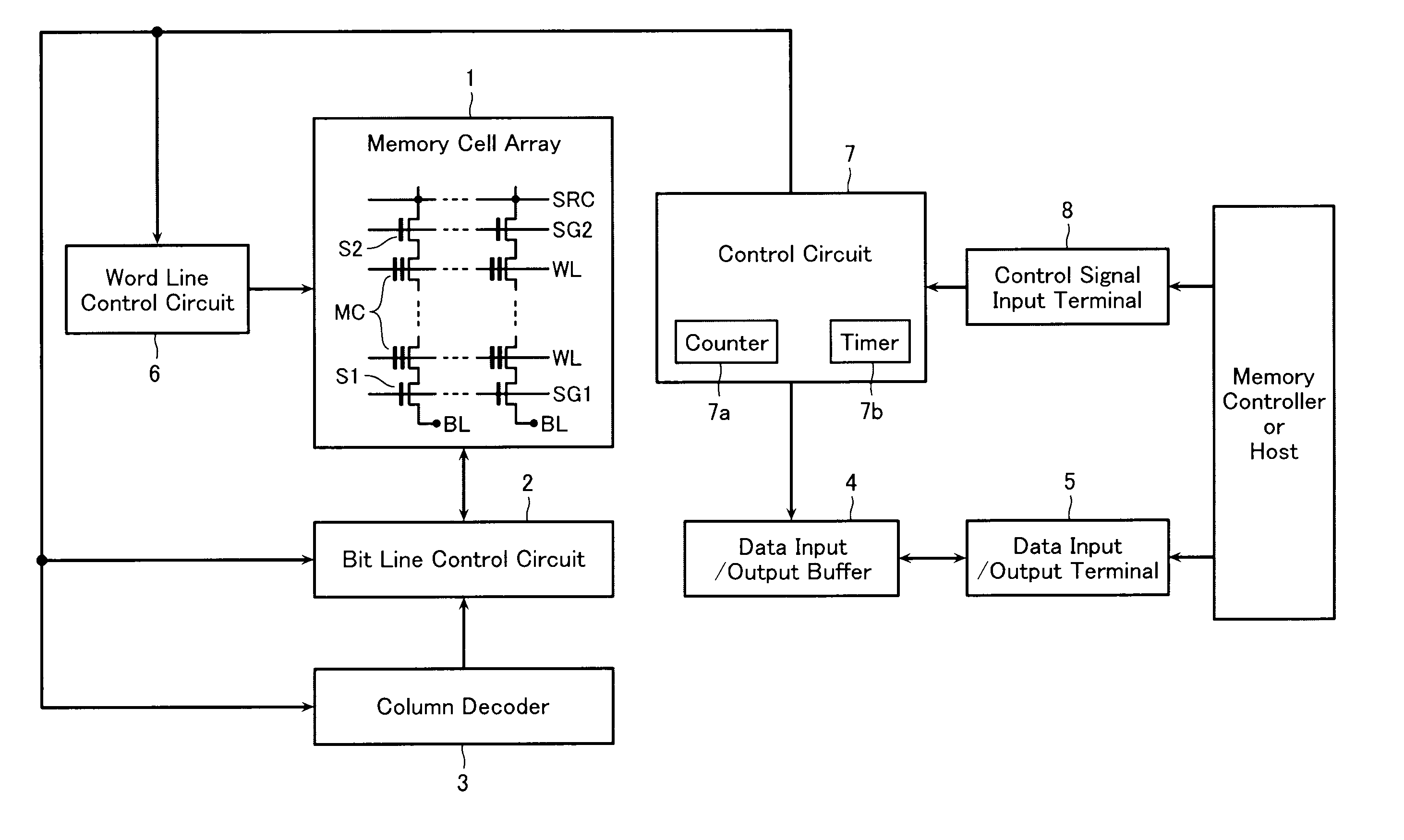
[0041]FIG. 1 is a block diagram showing a configuration of a nonvolatile semiconductor memory device according to a first embodiment. The nonvolatile semiconductor memory device is a NAND type flash memory employing a four-value storing system. The nonvolatile semiconductor memory device includes a memory cell array 1 configured by disposing memory cells MC for storing data in a matrix arrangement. The memory cell array 1 includes a plurality of bit lines BL, a plurality of word lines WL, a source line SRC, and a plurality of memory cells MC. The memory cells MC are electrically-rewritable, and disposed at the intersections of the bit lines BL and word lines WL in a matrix arrangement.

[0042]The memory cell array 1 is connected to a bit line control circuit 2 configured to control the voltages of the bit lines BL and a word line control circuit 6 configured to control the voltages of the word lines WL. That is, the bit line control circuit 2 reads data of a memor...

second embodiment

[0074]Next, a nonvolatile semiconductor memory device according to a second embodiment will be explained with reference to FIG. 11 and FIG. 12. The whole configuration of the nonvolatile semiconductor memory device according to the present embodiment is the same as the first embodiment, and hence a detailed explanation thereof will not be provided here. Further, any portions that are configured the same as the first embodiment will be denoted by the same reference numerals, and a redundant explanation thereof will not be provided.

[0075]In the second reading operation according to the first embodiment, a reading operation is executed by changing the voltage to be applied to the selected word line WL from the reading voltages BR or CR to the voltages BRs or CRs to execute a shift reading operation, and by not changing the reading voltage AR to the voltage ARs but instead raising the voltage of the source line SRC from 0 V to the voltage Vsrc. In contrast, in the second reading operati...

third embodiment

[0082]Next, a nonvolatile semiconductor memory device according to a third embodiment will be explained with reference to FIG. 13 to FIG. 17. The whole configuration of the nonvolatile semiconductor memory device according to the present embodiment is the same as the first embodiment, and hence a detailed explanation thereof will not be provided. Any portions that are configured the same as the first embodiment will be denoted by the same reference numerals, and a redundant explanation thereof will not be provided.

[0083]In the first and second embodiments, it is explained that the voltage to be applied to the source line SRC in the second reading operation is one type of voltage, that is, the voltage Vsrc. In contrast, according to the present embodiment, the voltage to be applied to the source line SRC in the second reading operation can be set to a plurality of positive values, for example, two positive values. Explanation will now be given with reference to FIG. 13 and FIG. 14.

[0...


PUM


Abstract

A nonvolatile semiconductor memory device according to one embodiment of the present invention includes: a memory cell array and a control circuit. The control circuit executes a first reading operation and a second reading operation. The first reading operation is an operation of reading a threshold voltage set in the selected memory cell by setting a voltage between a control gate electrode and source of the selected memory cell to a first value. The second reading operation is an operation of reading a threshold voltage set in the selected memory cell by setting a voltage between the control gate electrode and source of the selected memory cell to a second value lower than the first value. When executing the second reading operation, the control circuit keeps a voltage of the control gate electrode of the selected memory cell to 0 or a positive value.

Description

CROSS REFERENCE TO RELATED APPLICATION[0001]This application is based upon and claims the benefit of priority from prior Japanese Patent Application No. 2011-84762, filed on Apr. 6, 2011, the entire contents of which are incorporated herein by reference.BACKGROUND[0002]1. Field[0003]Embodiments described herein relate to an electrically-rewritable nonvolatile semiconductor memory device.[0004]2. Description of the Related Art[0005]A NAND type flash memory has a memory cell array which is configured by arranging memory strings each including a plurality of memory cells connected in series. Both ends of each memory string are connected to a bit line and a source line through select transistors respectively. The control gate electrodes of the memory cells of each memory string are connected to different word lines respectively. In each memory string, the plurality of memory cells are connected in series with sources and drains shared between them. The NAND type flash memory can have a ...

Claims


Application Information

Patent Timeline
Patent Type & Authority Applications(United States)
IPC IPC(8): G11C16/26
CPCG11C16/26G11C11/5628G11C16/349G11C16/3427G11C16/0483G11C16/08G11C16/10G11C16/14
Inventor SHIINO, YASUHIROTAKAHASHI, EIETSUUENO, KOKI
Owner KIOXIA CORP
Why Eureka
Try Eureka