Nitride semiconductor light emitting device

a light emitting device and semiconductor technology, applied in the direction of semiconductor devices, basic electric elements, electrical equipment, etc., can solve the problems of reducing the light emitting efficiency and reliability of the semiconductor light emitting device, and achieve the effects of improving current distribution, light emitting efficiency, and enhancing current injection

Active Publication Date: 2012-10-18
SAMSUNG ELECTRONICS CO LTD
View PDF2 Cites 22 Cited by
  • Summary
  • Abstract
  • Description
  • Claims
  • Application Information

AI Technical Summary

Benefits of technology

[0007]An aspect of the present invention provides a nitride semiconductor light emitting device being improved in current distribution due to two-dimensional electron gas (2DEG) and having an enhanced current injection effect and light emitting efficiency.
[0008]An aspect of the present invention also provides a nitride semiconductor light emitting device having an electron injection layer relieving stress from a nitride layer and reducing the possibility of occurrence of defects.
[0009]An aspect of the present invention also provides a nitride semiconductor light emitting device having superior luminance and being improved in productivity by simplifying a nitride semiconductor structure and reducing production time.
[0017]At least one of the first and second layers may have a reduced energy band gap in the individual multilayer structures in the direction toward the active layer.
[0026]At least one of the first and second layers may have a reduced energy band gap in the individual multilayer structures in the direction toward the active layer.

Problems solved by technology

However, such a complex stack structure may increase stress and the possibility of occurrence of defects in an interface, and defects may be propagated to the active layer, whereby light emitting efficiency and reliability of the semiconductor light emitting device may be reduced.

Method used


Image

  • Nitride semiconductor light emitting device
  • Nitride semiconductor light emitting device
  • Nitride semiconductor light emitting device

Examples


first embodiment

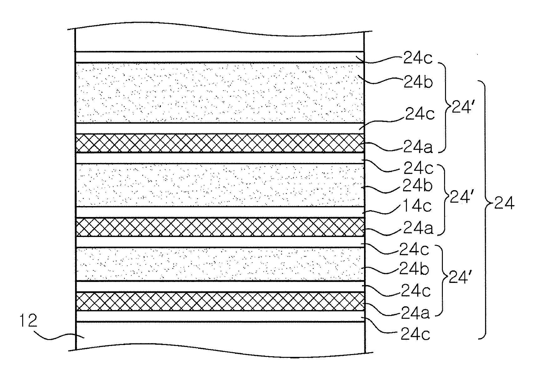
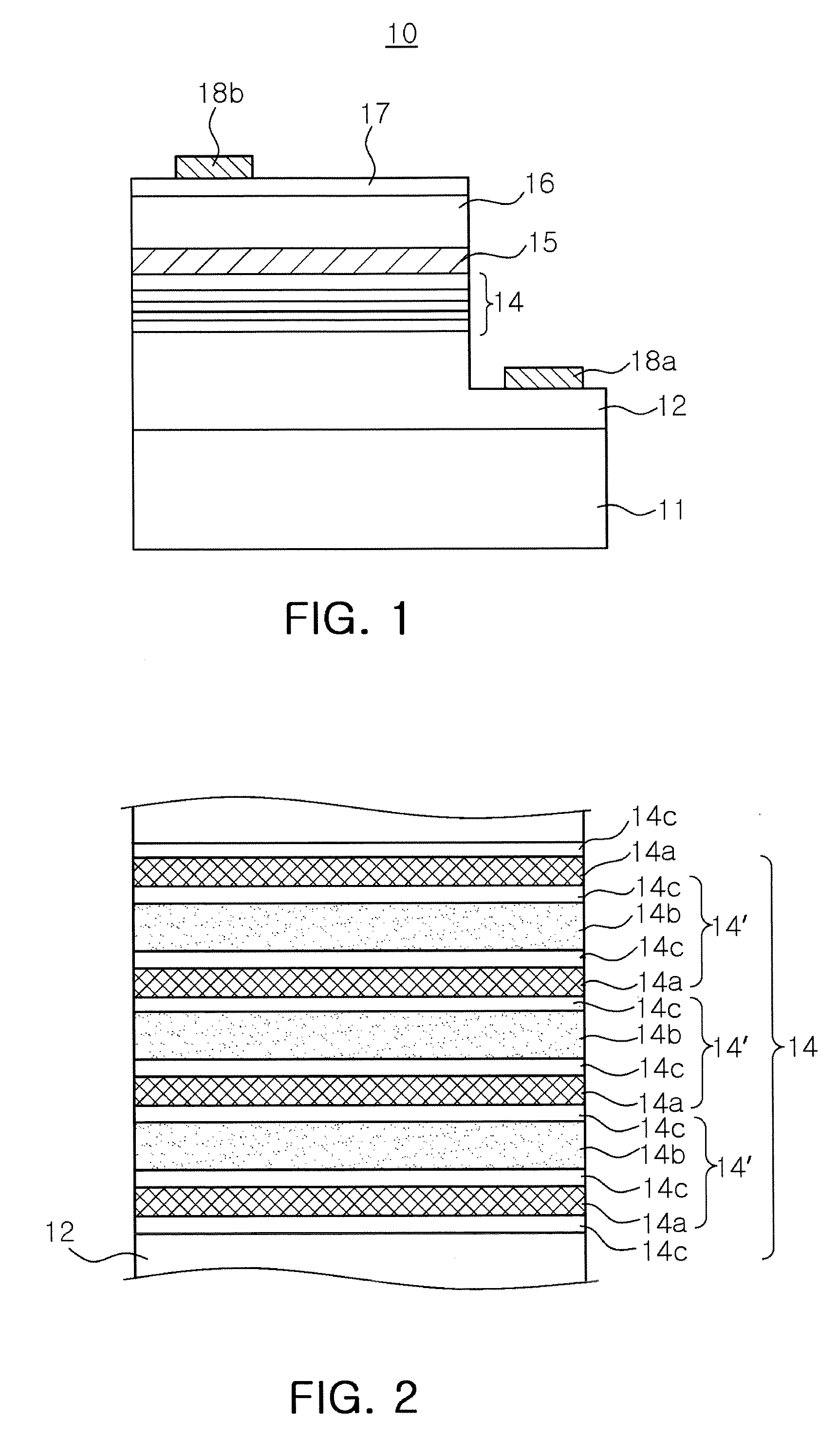
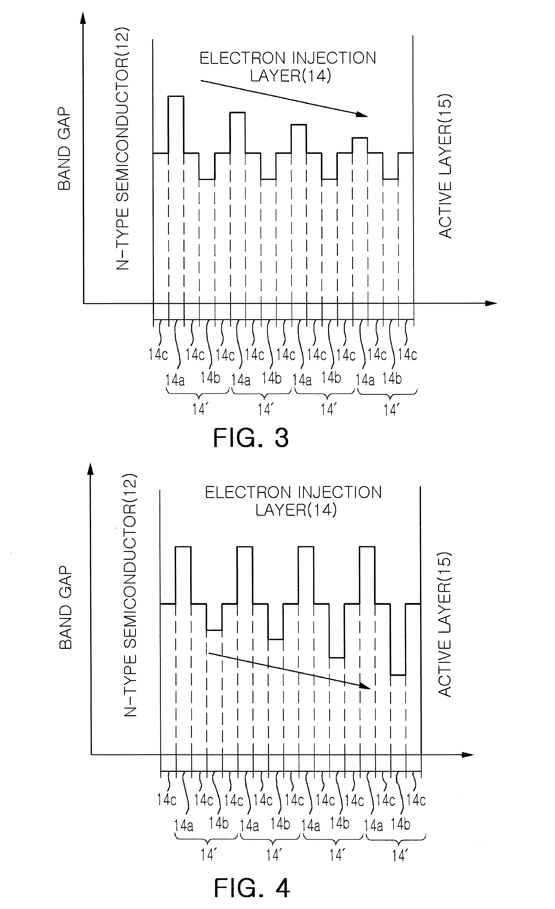
[0055]FIG. 4 is a graph illustrating another example of a band gap profile of the electron injection layer applicable to the present invention. Unlike the embodiment depicted in FIG. 3, the second layer 14b having the lowest energy band gap among the first to third layers 14a, 14b and 14c may have a reduced energy band gap in the individual multilayer structures 14′ in a direction toward the active layer 15, and the energy band gaps of the first and third layers 14a and 14c may be maintained in the entirety of the electron injection layer 14. In this case, electron injection from the n-type nitride semiconductor layer 12 to the active layer 15 may be facilitated to thereby improve electron injection efficiency. Unlike the present embodiment, all the energy band gaps of the first to third layers 14a, 14b and 14c may have a sloped structure. Alternatively, the energy band gaps of two layers may have a sloped structure and the energy band gap of one layer may be consistently maintained...

second embodiment

[0061]FIG. 7 is a graph illustrating another example of a band gap profile of the electron injection layer according to the present invention. Unlike the embodiment depicted in FIG. 6, at least one layer in multilayer structures 34′ of an electron injection layer 34 according to this embodiment may have a reduced energy band gap in the individual multilayer structures 34′ in a direction toward the active layer 15. That is, due to a sloped structure in which the energy band gap of the at least one layer is reduced in the individual multilayer structures 34′ in a direction toward the active layer 15 while the thickness of the layer having the lowest energy band gap is increased in the individual multilayer structures 34′ in a direction toward the active layer 15, electron injection efficiency from the n-type nitride semiconductor layer 12 to the active layer 15 may be significantly improved.

[0062]With reference to FIG. 7, as described in the electron injection layer 24 of FIG. 6, each...


PUM


Abstract

There is provided a nitride semiconductor light emitting device including: n-type and p-type nitride semiconductor layers; an active layer disposed between the n-type and p-type nitride semiconductor layers; and an electron injection layer disposed between the n-type nitride semiconductor layer and the active layer. The electron injection layer has a multilayer structure, in which three or more layers having different energy band gaps are stacked, and the multilayer structure is repetitively stacked at least twice. At least one layer among the three or more layers has a reduced energy band gap in individual multilayer structures in a direction toward the active layer, and the layer having the lowest energy band gap has an increased thickness in individual multilayer structures in a direction toward the active layer.

Description

CROSS-REFERENCE TO RELATED APPLICATIONS[0001]This application claims the priority of Korean Patent Application No. 10-2011-0034401 filed on Apr. 13, 2011, in the Korean Intellectual Property Office, the disclosure of which is incorporated herein by reference.BACKGROUND OF THE INVENTION[0002]1. Field of the Invention[0003]The present invention relates to a nitride semiconductor light emitting device.[0004]2. Description of the Related Art[0005]In recent years, a group III-V nitride semiconductor, such as a GaN semiconductor, has been prominent as an essential material for light emitting devices, such as light emitting diodes (LEDs), laser diodes (LDs), and the like, due to its excellent physical and chemical properties. LEDs or LDs using a group III-V nitride semiconductor material are mainly used in light emitting devices for producing light in a blue or green wavelength band. These light emitting devices are being used as light sources for various applications requiring high curren...

Claims


Application Information

Patent Timeline
Patent Type & Authority Applications(United States)
IPC IPC(8): H01L33/32
CPCH01L33/32H01L33/04
Inventor SHIM, HYUN WOOKYOON, SUK HOSAKONG, TANKIM, JE WONKIM, KI SUNG
Owner SAMSUNG ELECTRONICS CO LTD
Why Eureka
Try Eureka