
Power ldmos device and high voltage device

Active Publication Date: 2012-10-18
EPISIL TECH
View PDF2 Cites 3 Cited by
  • Summary
  • Abstract
  • Description
  • Claims
  • Application Information

AI Technical Summary

Benefits of technology

[0007]Accordingly, the present invention provides a high voltage device (e.g. a power LDMOS device) to effectively reduce the area of the terminal region of the device and further enhance the degree of integration of the same.
[0029]In view of the above, in a high voltage device (e.g. a power LDMOS device), excessive electric field around ends or corner portions can be effectively lessened by disposing at least one trench insulating structure in the terminal region. Further, in the terminal region of the present invention, the vertical distance from the ends of the drain regions to the periphery of the source region in the terminal region can be reduced from more than 80 μm to 0-50 μm. Accordingly, the design rule for the terminal region can be effectively reduced, the area of the terminal region of the device can be decreased, and the degree of integration of the device can be further enhanced.

Problems solved by technology

However, this method would waste a significant amount of area and reduce the competitiveness.

Method used


Image

  • Power ldmos device and high voltage device
  • Power ldmos device and high voltage device
  • Power ldmos device and high voltage device

Examples


first embodiment

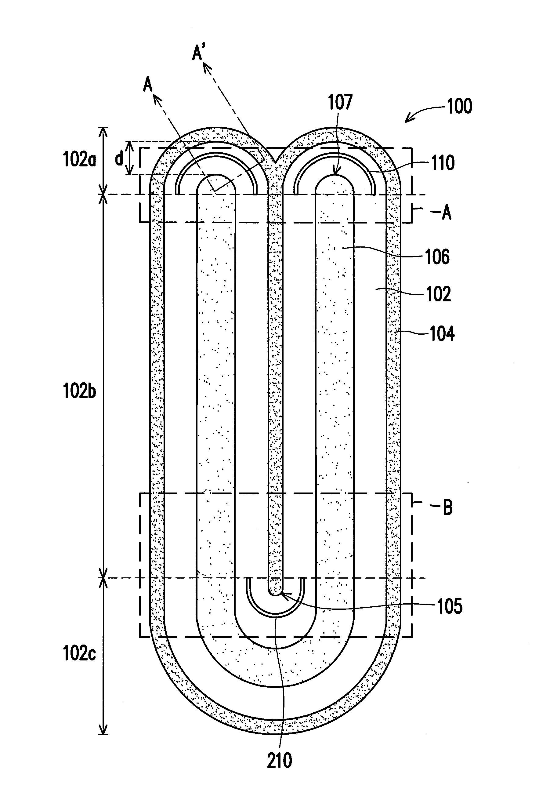
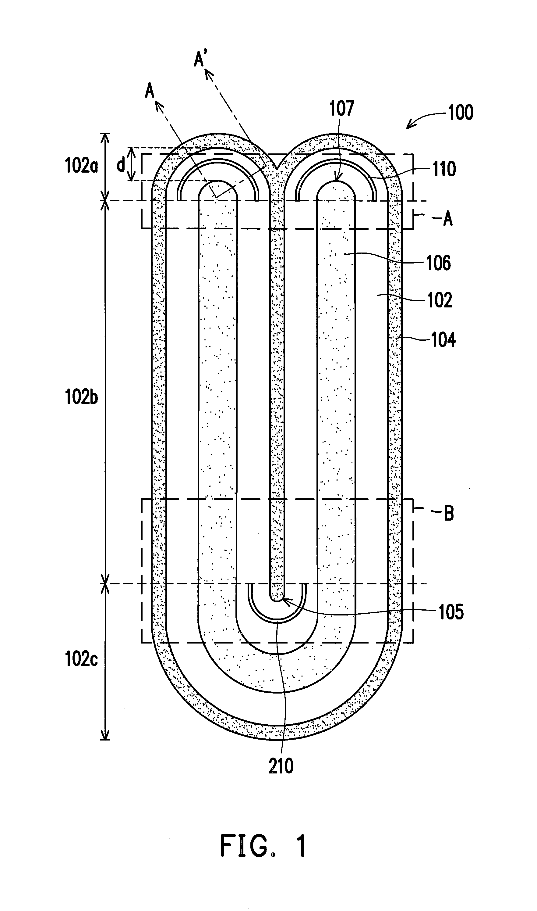
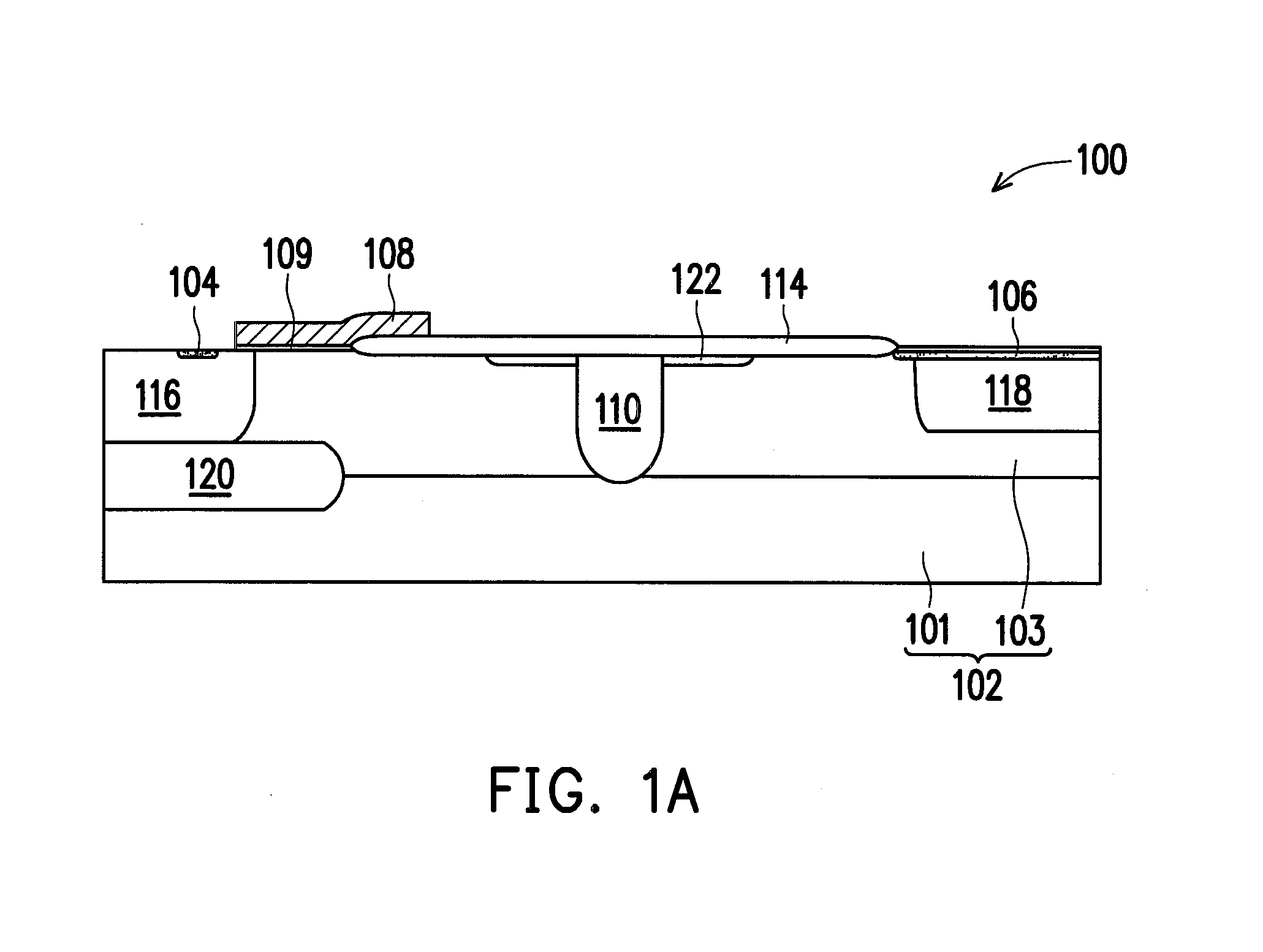
[0038]FIG. 1 schematically illustrates a top view of a power LDMOS device according to a first embodiment of the present invention. FIG. 1A schematically illustrates a cross-sectional view taken along the line A-A′ in FIG. 1. For clarity and convenience of illustration, only source regions, drain regions and trench insulating structures are shown in FIG. 1.

[0039]Referring to FIGS. 1 and 1A, a power LDMOS device 100 of the first embodiment includes a substrate 102, a plurality of source regions 104 each having a stripe shape, a plurality of drain regions 106 each having a stripe shape, a plurality of gates 108, a plurality of trench insulating structures 110 and a plurality of trench insulating structures 210.

[0040]The substrate 102 includes a wafer substrate layer 101 and an epitaxial layer 103 disposed on the wafer substrate layer 101. The wafer substrate layer 101 is a P-type layer, and the epitaxial layer 103 is an N-type epitaxial layer, for example. The substrate 102 has a fing...

second embodiment

[0056]FIG. 3 schematically illustrates a top view of a power LDMOS device according to a second embodiment of the present invention. For clarity and convenience of illustration, only source regions, drain regions and trench insulating structures are shown in FIG. 3. The power LDMOS device of the second embodiment is similar to that of the first embodiment. The differences between them are described in the following, and the same parts are not iterated therein.

[0057]Referring to FIG. 3, a power LDMOS device 200 of the second embodiment includes a substrate 102, a plurality of source regions 104 each having a stripe shape, a plurality of drain regions 106 each having a stripe shape, a plurality of gates 108, a plurality of trench insulating structures 110, a plurality of trench insulating structures 210, a plurality of trench insulating structures 310 and a plurality of trench insulating structures 410.

[0058]The trench insulating structures 110 are disposed in the substrate 102 in the...


PUM


Abstract

A power LDMOS device including a substrate, source and drain regions, gates and trench insulating structures is provided. The substrate has a finger tip area, a finger body area and a palm area. The source regions are in the substrate in the finger body area and further extend to the finger tip area. The neighboring source regions in the finger tip area are connected. The outmost two source regions further extend to the palm area and are connected. The drain regions are in the substrate in the finger body area and further extend to the palm area. The neighboring drain regions in the palm area are connected. The source and drain regions are disposed alternately. A gate is disposed between the neighboring source and drain regions. The trench insulating structures are in the substrate in the palm area and respectively surround ends of the drain regions.

Description

CROSS-REFERENCE TO RELATED APPLICATION[0001]This application claims the priority benefit of Taiwan application serial no. 100113398, filed Apr. 18, 2011. The entirety of the above-mentioned patent application is hereby incorporated by reference herein and made a part of this specification.BACKGROUND OF THE INVENTION[0002]1. Field of Invention[0003]The present invention relates to a high voltage (>400V) device, and more generally to a power lateral double diffusion MOS (power LDMOS) device having a smaller terminal region.[0004]2. Description of Related Art[0005]As the semiconductor industry is developed with time, a high voltage device such as a power LDMOS device has been widely applied in many electronic systems. Generally speaking, a power LDMOS device includes a plurality of source regions, a plurality of drain regions and a plurality of gates. The source regions and the drain regions are disposed alternately. A gate is disposed between the neighboring source and drain region...

Claims


Application Information

Patent Timeline
IPC IPC(8): H01L29/78
CPCH01L29/0634H01L29/0653H01L29/7816H01L29/1095H01L29/42368H01L29/0696
Inventor LEE, CHUNG-YEHWU, PEI-HSUNHUANG, SHIANG-WEN
Owner EPISIL TECH
Learn More