Method of Selective Photo-Enhanced Wet Oxidation for Nitride Layer Regrowth on Substrates

a technology of nitride and wet oxidation, which is applied in the direction of semiconductor/solid-state device manufacturing, semiconductor devices, electrical devices, etc., can solve the problems of serious material contamination issues to the growth of nitride layers thereafter, and the efficiency and technological maturity of ingan-gan blue/green devices have not yet been reached, so as to achieve high bandgap energy

Active Publication Date: 2012-10-18
OPTO TECH
View PDF1 Cites 10 Cited by
  • Summary
  • Abstract
  • Description
  • Claims
  • Application Information

AI Technical Summary

Benefits of technology

[0019]In another aspect, a method may comprise: forming a first III-nitride layer with a first low bandgap energy on a first surface of a C plane (0001) sapphire substrate; forming a second III-nitride layer with a first high bandgap energy on the first III-nitride layer; forming an LED structure over the second III-nitride layer; and forming, at least in part by selective photo-enhanced oxidation, in the LED structure a plurality of air gaps that are parallel to one another and adjacent the second III-nitride layer.
[0020]In one embodiment, forming, at least in part by selective photo-enhanced oxidation, a plurality of air gaps that are parallel to one another and adjacent the second III-nitride layer may comprise: transforming portions of a surface of the second III-nitride layer into a plurality of III-oxide stripes by photo-enhanced wet oxidation; forming a plurality of III-nitride nanowires with a second low bandgap energy on the second III-nitride layer between the III-oxide stripes; selectively transforming at least some of the III-nitride nanowires into III-oxide nanowires by selective photo-enhanced oxidation; forming a third III-nitride layer on the second III-nitride layer and over the III-oxide nanowires; and removing the III-oxide nanowires to form the plurality of air gaps.

Problems solved by technology

AIGaN (aluminum gallium nitride) of varying AIN molar fraction can be used to manufacture the cladding and quantum well layers for ultraviolet LEDs, but these devices have not yet reached the level of efficiency and technological maturity of the InGaN-GaN blue / green devices.
However, impurity migration from the mask region (Si02) can cause serious material contamination issues to the growth of nitride layers thereafter.
However, as with the aforementioned approach, impurity migration from the SiO2 mask region can cause serious material contamination issues to the growth of nitride layers thereafter.
Screw dislocations, which are undesirable, tend to exist at the bottom of the V-notch grooves.
However, such techniques may result in undesirable impurity migration and / or damage to the crystal atomic structure.

Method used


Image

  • Method of Selective Photo-Enhanced Wet Oxidation for Nitride Layer Regrowth on Substrates
  • Method of Selective Photo-Enhanced Wet Oxidation for Nitride Layer Regrowth on Substrates
  • Method of Selective Photo-Enhanced Wet Oxidation for Nitride Layer Regrowth on Substrates

Examples


Embodiment Construction

Overview

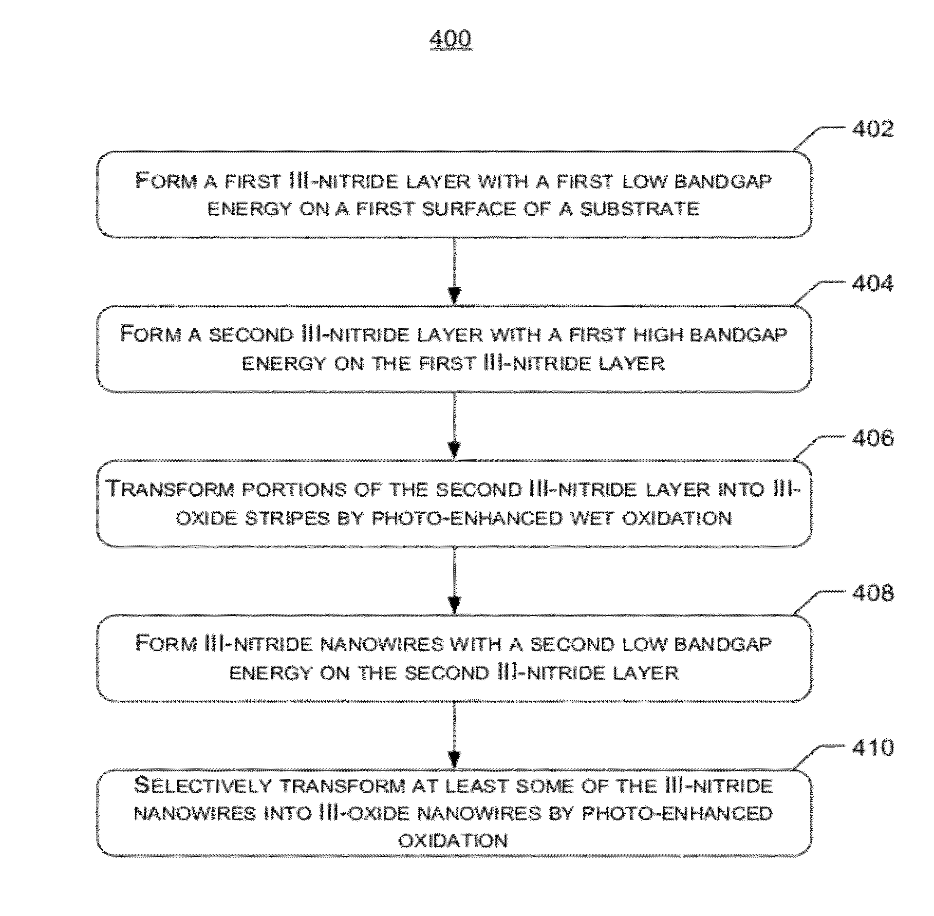
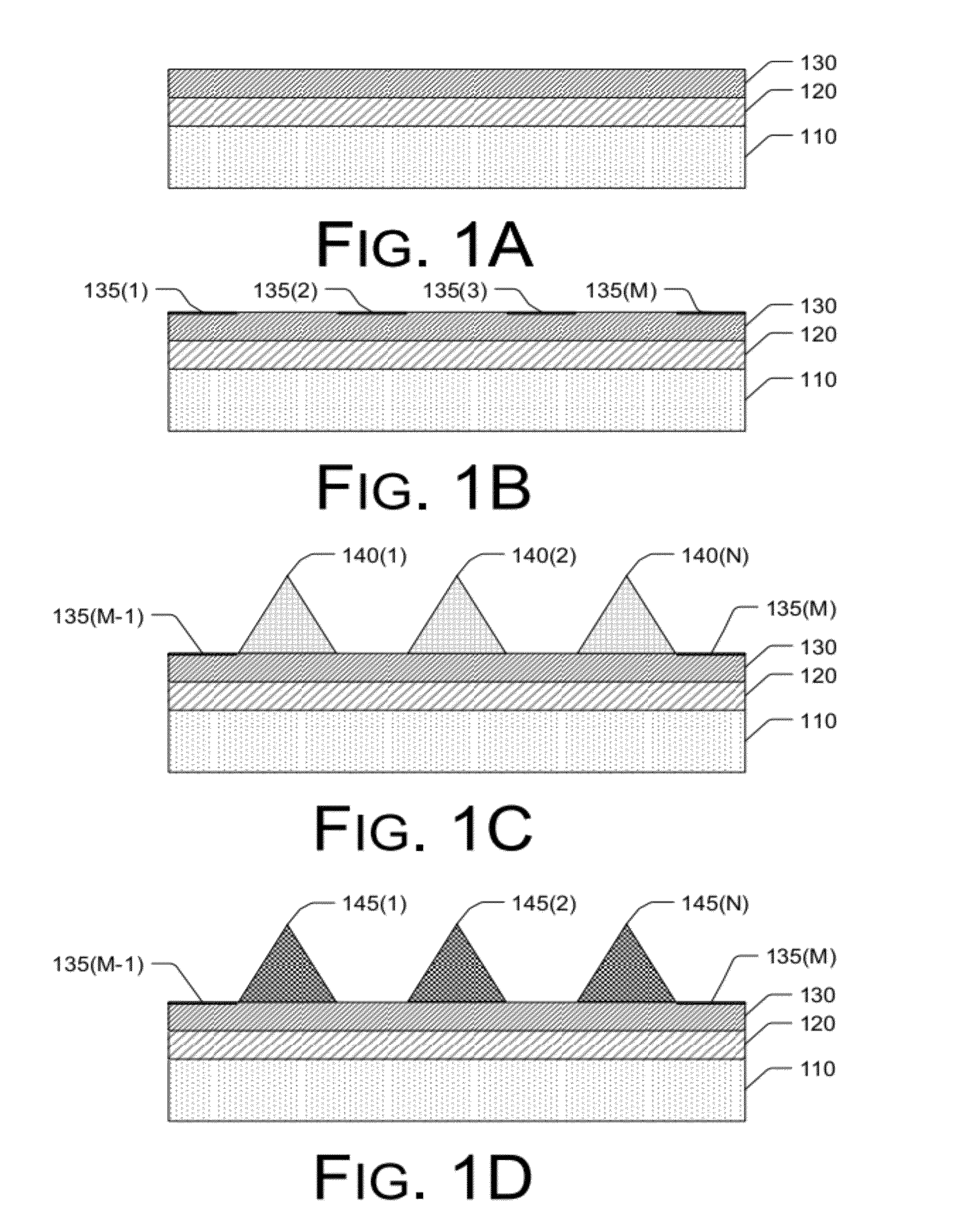
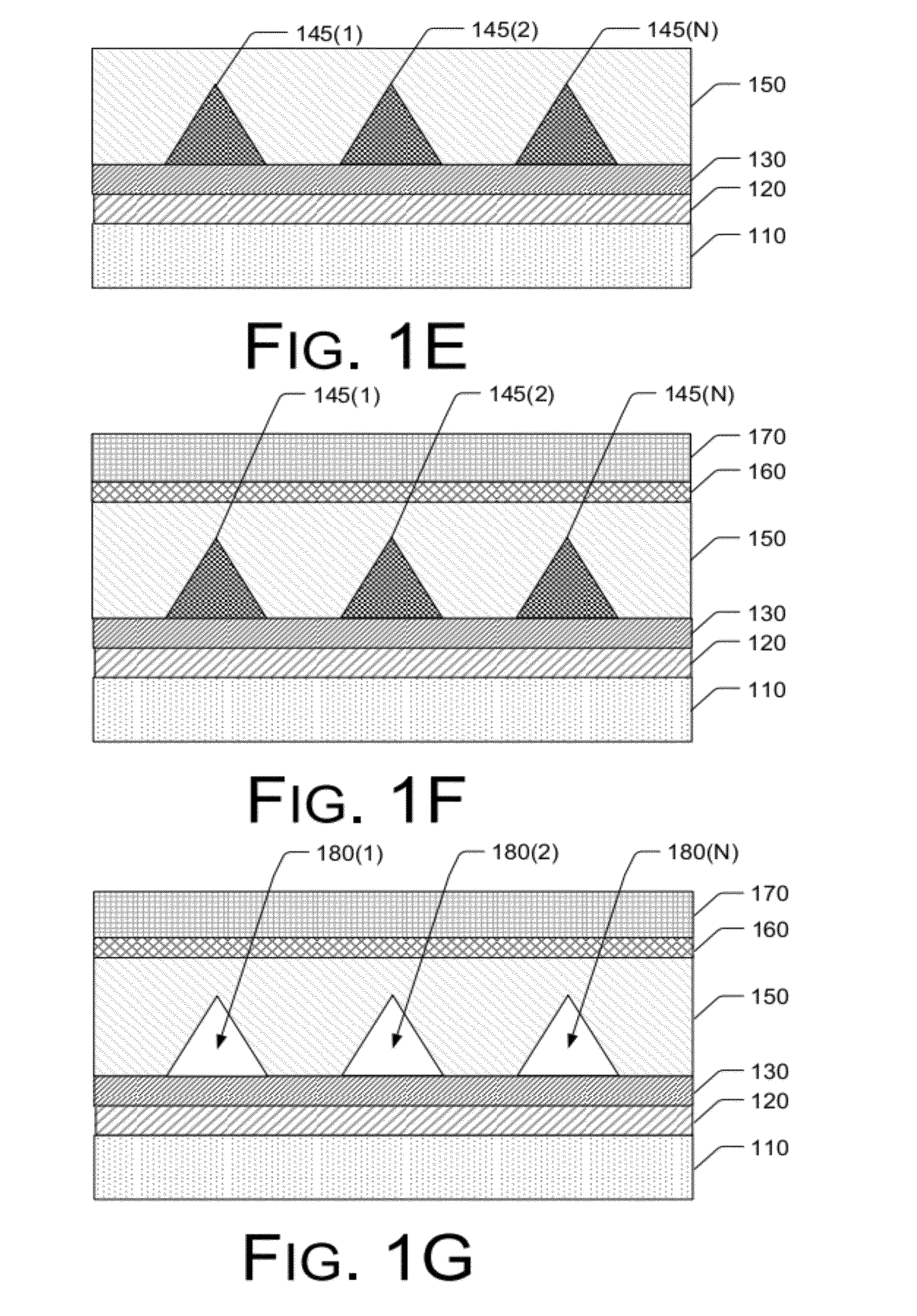
[0037]Various embodiments of the present disclosure pertain to techniques of selective photo-enhanced wet oxidation in fabrication of LED structures and in suppression of propagation of screw dislocations in LED structures.

[0038]In a semiconductor structure where a layer of III-nitride with low bandgap energy Eg,Lo and a layer of III-nitride with high bandgap energy Eg,Hi are deposited one above the other, selective photo-enhanced wet oxidation with a photonic energy hγ, where Eg,Log,Hi, can transform III-nitride compounds with Eg,Lo into III-oxide compounds. This technique can be utilized to form III-oxide nanowires over the layers of III-nitride. Lateral expitaxy of a new layer of III-nitride over the existing layers of III-nitride and III-oxide nanowires can then be achieved by MOCVD. Afterwards, air gaps can be formed by dissolving the III-oxide nanowires using an acidic electrolyte or a basic electrolyte. The air gaps provide crystal lattice momentum for optical diffrac...


PUM

PropertyMeasurementUnit
wavelengthsaaaaaaaaaa
inclined angleaaaaaaaaaa

Abstract

Various embodiments of the present disclosure pertain to selective photo-enhanced wet oxidation for nitride layer regrowth on substrates. In one aspect, a method may comprise: forming a first III-nitride layer with a first low bandgap energy on a first surface of a substrate; forming a second III-nitride layer with a first high bandgap energy on the first III-nitride layer; transforming portions of the first III-nitride layer into a plurality of III-oxide stripes by photo-enhanced wet oxidation; forming a plurality of III-nitride nanowires with a second low bandgap energy on the second III-nitride layer between the III-oxide stripes; and selectively transforming at least some of the III-nitride nanowires into III-oxide nanowires by selective photo-enhanced oxidation.

Description

BACKGROUND[0001]1. Technical Field[0002]Various embodiments of the present disclosure relate to semiconductor light-emitting devices and, more particularly, to a method of selective photo-enhanced wet oxidation for nitride layer regrowth on substrates.[0003]2. Description of the Relevant Art[0004]Light-emitting diodes (LEDs) are a type of semiconductor-based light source. An LED typically includes semiconducting materials doped with impurities to create a p-n junction. The wavelength of the light emitted, and thus its color, depends on the bandgap energy of the materials forming the p-n junction. In silicon or germanium diodes, the electrons and holes recombined by a non-radiative transition produce no optical emission, because these are indirect bandgap materials. The materials used for the LED have a direct bandgap with energies corresponding to near-infrared, visible or near-ultraviolet light. LEDs are usually built on an n-type substrate with an electrode attached to the p-type ...

Claims


Application Information

Patent Timeline
Patent Type & Authority Applications(United States)
IPC IPC(8): H01L31/18H01L21/205
CPCH01L21/0242H01L21/02458H01L21/0254H01L33/32H01L21/02639H01L33/007H01L33/06H01L21/02603
Inventor PENG, LUNG-HANYU, JENG-WEIYEH, PO-CHUN
Owner OPTO TECH
Why Eureka
Try Eureka