Integrated optical device and manufacturing method of the same

Active Publication Date: 2013-03-14
FURUKAWA ELECTRIC CO LTD
View PDF5 Cites 4 Cited by
  • Summary
  • Abstract
  • Description
  • Claims
  • Application Information

AI Technical Summary

Benefits of technology

[0012]According to a first aspect of the present invention, provided is an optical integrated device comprising a first waveguide that is formed on a substrate and includes a first optical path; an electrode formed on the first waveguide; a second waveguide that is formed on the substrate and includes a second optical path; and a transparent waveguide that is formed on the substrate between the first wavegu

Problems solved by technology

However, when current flows from the electrode of the optically active element to the interface between the optically active element and the other element, generation and propagation of crystal defects is promoted.
These crystal defects degrade the characteristics of the elements and decrease the reliability of the optical integrated device, particularly for the optically active elements.
However, when the offset amount of the electrode is too small, the current flowing through the interface between the optically active element and th

Method used


Image

  • Integrated optical device and manufacturing method of the same
  • Integrated optical device and manufacturing method of the same
  • Integrated optical device and manufacturing method of the same

Examples


first embodiment

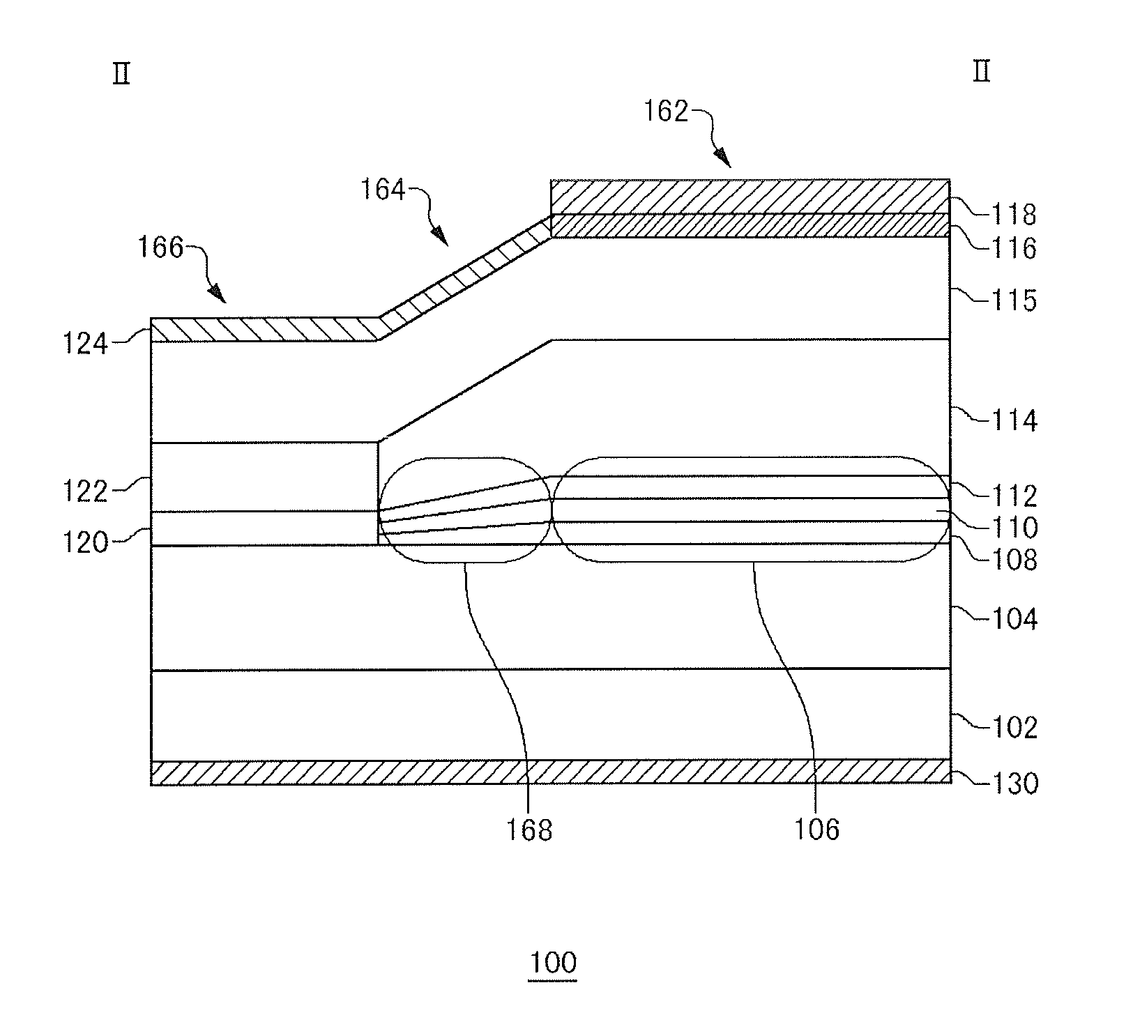
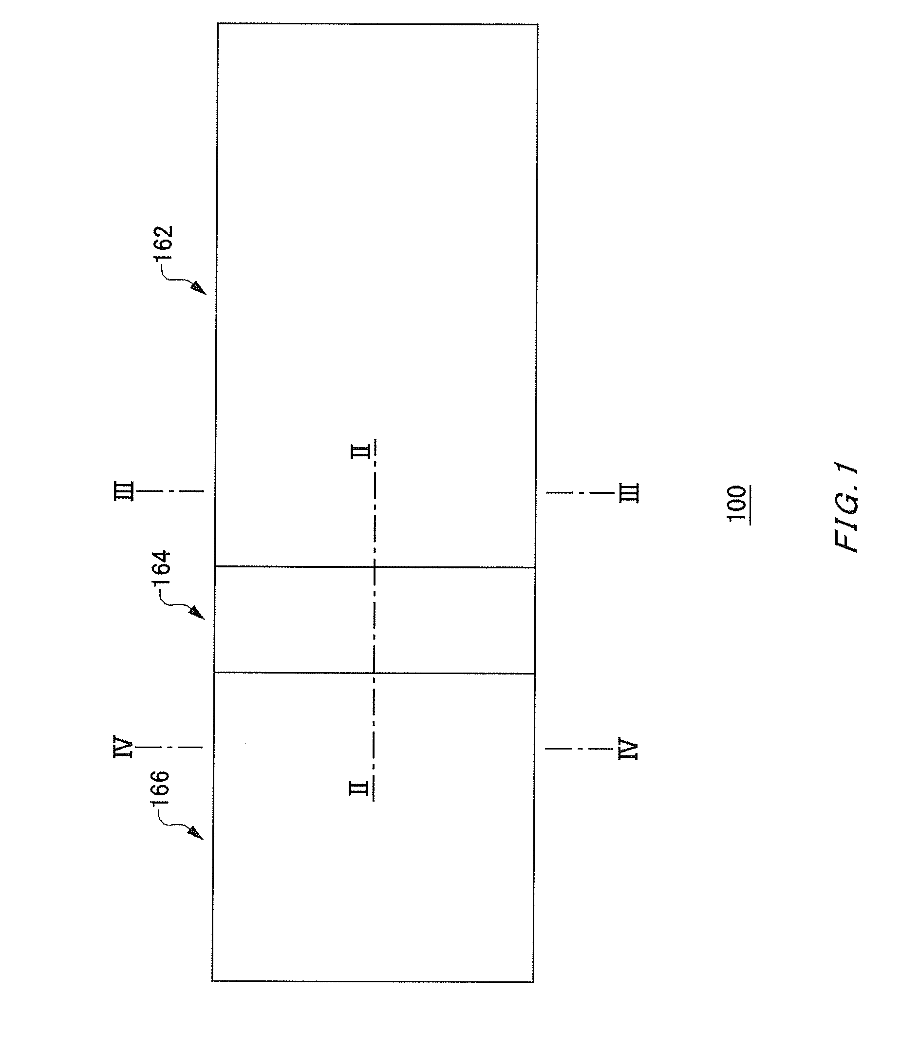
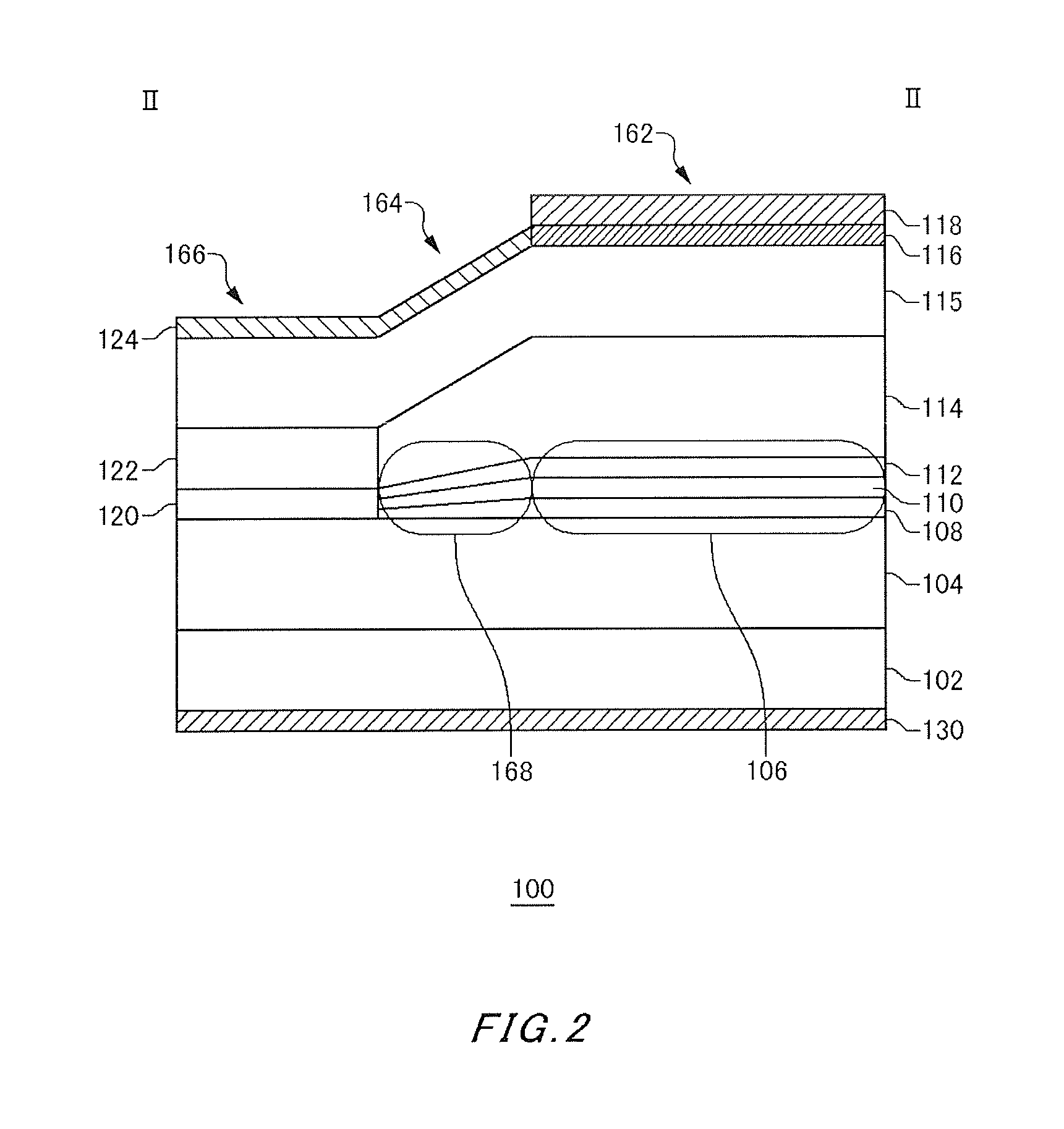
[0031]FIG. 1 is a schematic overhead view of an optical integrated device 100 according to the present invention. The optical integrated device 100 includes a semiconductor laser 162, a transparent waveguide 164, and an optical waveguide 166. The semiconductor laser 162 emits laser light. The oscillation wavelength of the primary-mode laser light of the semiconductor laser 162 may be 1310 nm or 1550 nm, for example. The transparent waveguide 164 is coupled to the semiconductor laser 162. The optical waveguide 166 is coupled to the transparent waveguide 164. The laser light emitted by the semiconductor laser 162 is guided to the optical waveguide 166 through the transparent waveguide 164.

[0032]FIG. 2 is a schematic cross-sectional view of the semiconductor laser 162, the transparent waveguide 164, and the optical waveguide 166 of the optical integrated device 100 according to the first embodiment, over the line II-II of FIG. 1. The semiconductor laser 162 includes a substrate 102, a ...

second embodiment

[0079]FIG. 12 is a schematic cross-sectional view of the semiconductor laser 162, a transparent waveguide 264, and the optical waveguide 166 of an optical integrated device 200 according to the present invention. In FIG. 12, components that have the same function and configuration as components in FIG. 2 may be given the same reference numerals. The optical integrated device 200 has the same overhead view as the optical integrated device 100 shown in FIG. 1, and FIG. 7 is a schematic cross-sectional view of the optical integrated device 200 over the II-II of FIG. 1. The semiconductor laser 162 and the optical waveguide 166 of the optical integrated device 200 may each have the cross sections shown in FIGS. 3 and 4, in the same manner as in the optical integrated device 100.

[0080]The semiconductor laser 162 includes the substrate 102, the lower cladding layer 104, the active layer 106, the upper cladding layer 114, the p-InP layer 115, the contact layer 116, the p-side electrode 118,...

third embodiment

[0093]FIG. 15 is a schematic cross-sectional view of the semiconductor laser 162, the transparent waveguide 164, and the optical waveguide 166 of an optical integrated device 300 according to the present invention. In FIG. 15, components having the same function and configuration as components shown in FIG. 2 are given the same reference numerals. Further, the optical integrated device 300 has the same overhead view as the optical integrated device 100 shown in FIG. 1, and FIG. 15 is a schematic cross-sectional view of the optical integrated device 300 over the II-II of FIG. 1. The semiconductor laser 162 and the optical waveguide 166 of the optical integrated device 300 may each have the cross sections shown in FIGS. 3 and 4, in the same manner as in the optical integrated device 100.

[0094]The semiconductor laser 162 includes the substrate 102, the lower cladding layer 104, the active layer 106, the upper cladding layer 114, the p-InP layer 115, the contact layer 116, the p-side el...


PUM


Abstract

Provided is an optical integrated device comprising a first waveguide that is formed on a substrate and includes a first optical path; an electrode formed on the first waveguide; a second waveguide that is formed on the substrate and includes a second optical path; and a transparent waveguide that is formed on the substrate between the first waveguide and the second waveguide, and includes a transparent core that serves as an optical path and is formed of a material having higher bandgap energy than the first optical path. The electrode is formed above the first waveguide and is not formed above the transparent waveguide, and elements including the first waveguide are optically active elements that operate according to current injected thereto.

Description

[0001]The contents of the following Japanese patent applications are incorporated herein by reference:[0002]NO. 2011-196151 filed on Sep. 8, 2011, and[0003]NO. 2012-149952 filed on Jul. 3, 2012.BACKGROUND[0004]1. Technical Field[0005]The present invention relates to an optical integrated device and an optical integrated device manufacturing method.[0006]2.Related Art[0007]An optical integrated device is known in which a semiconductor laser, an optical waveguide, and a modulator are integrated monolithically on a single substrate, as shown in Patent Document 1, for example.[0008]Patent Document 1: K. Shinoda, et al., “Highly reliable operation of InGaAlAs / InGaAsP integrated lasers,” Indium Phosphide & Related Materials, 2007. IPRM '07. IEEE 19th International Conference, IEEE, May 2007, pp. 39-42[0009]In a monolithic integrated optical integrated device, there is a region where an optically active element that includes an electrode, such as a semiconductor laser, is coupled to anothe...

Claims


Application Information

Patent Timeline
IPC IPC(8): G02B6/12H01L33/58
CPCB82Y20/00H01S5/0612H01S5/026H01S5/34306H01S5/2063H01S5/02453G02B6/1228H01S5/106G02B6/12004H01S5/227
Inventor IWAI, NORIHIROISHII, HIROTATSU
Owner FURUKAWA ELECTRIC CO LTD
Why Eureka
Try Eureka