Buffer layers for rebco films for use in superconducting devices

a buffer layer and film technology, applied in the field of superconducting materials, can solve the problems of destroying superconductive properties, difficult to deposit high-quality buffer layers using low-cost processes, and a substantial part of the total conductor cost of buffer deposition

Inactive Publication Date: 2012-10-18
UNIV OF TENNESSEE RES FOUND +1
View PDF5 Cites 16 Cited by
  • Summary
  • Abstract
  • Description
  • Claims
  • Application Information

AI Technical Summary

Problems solved by technology

It is now clear that while it is fairly straightforward to fabricate long lengths of biaxially textured metals or alloys, it is quite difficult to deposit high quality buffer layers using low cost processes.
Nickel can poison the YBCO layer, destroying the superconductive properties.
Even though the buffer layers are much thinner than the YBCO layer, buffer deposition cost is a substantial part of the total conductor cost.
Most of such oxide layers do not offer the bi-axial cubic texture required for high critical currents in the HTS layer.
Uncontrolled growth of substrate oxides, however, can result in multiple failures.
Rapid and inhomogeneous oxide growth can penetrate the buffer layers and cause deterioration of the barrier properties of the buffer layer.
However, when the CeO2 layer is grown greater than 0.2 μm in thickness, it readily forms micro-cracks.
Many buffer layer materials or substrates exhibit a deleterious chemical reactivity toward the precursor layer during the ex situ anneal to the extent that a high-Jc epitaxial YBCO film cannot be obtained.

Method used


Image

  • Buffer layers for rebco films for use in superconducting devices
  • Buffer layers for rebco films for use in superconducting devices
  • Buffer layers for rebco films for use in superconducting devices

Examples


Embodiment Construction

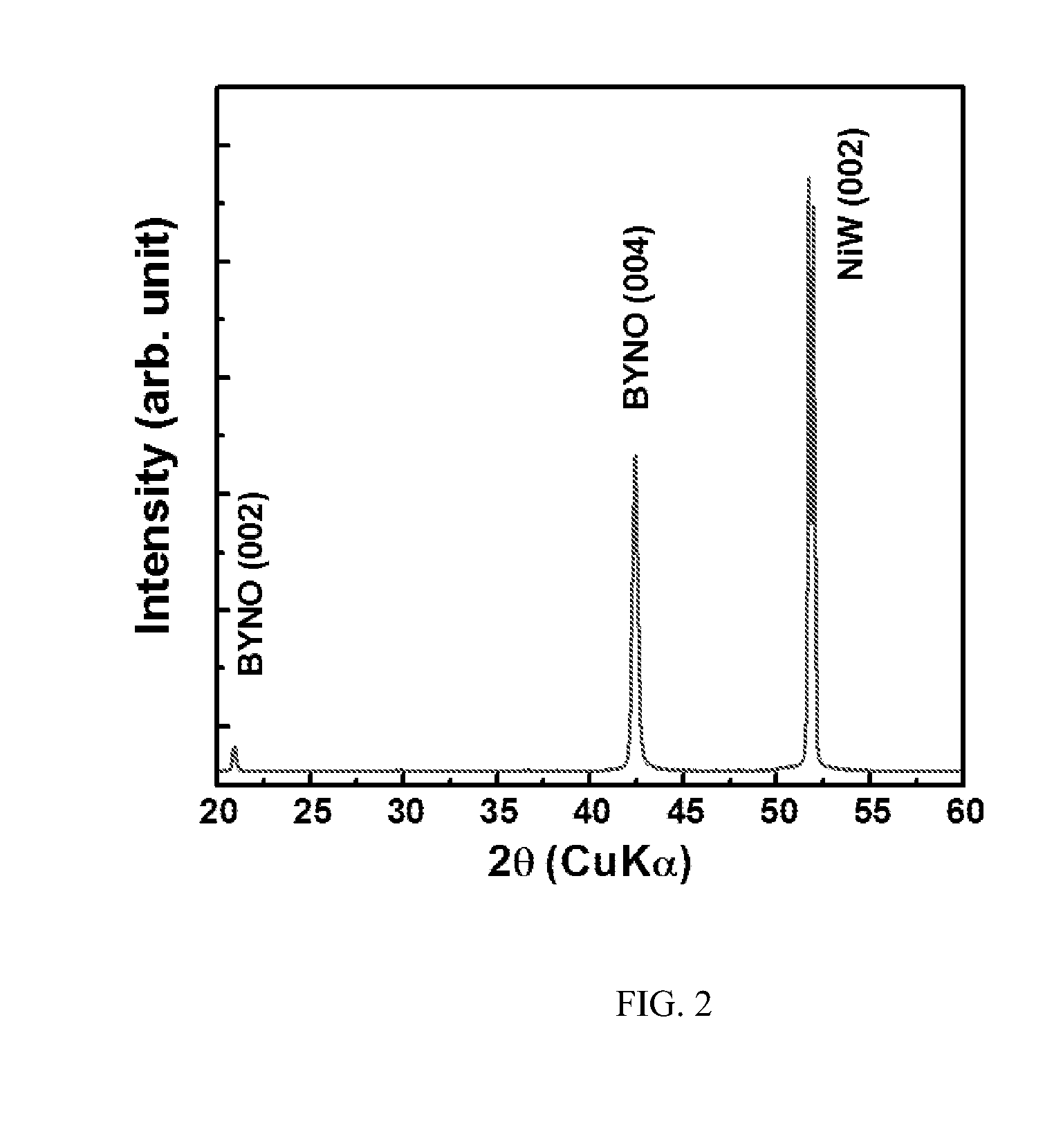
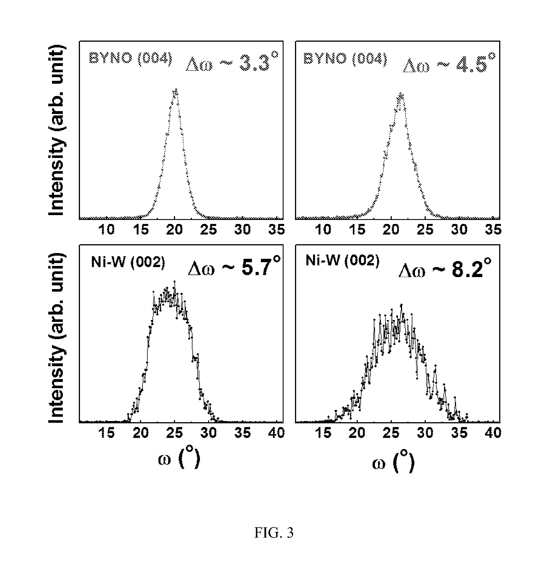
[0033]Superconducting articles according to the invention include a double perovskite buffer layer, which can be a cap layer, a biaxially textured substrate and a biaxially textured superconducting layer. The term “cap layer” as used herein means that the double perovskite layer is in physical contact with the superconducting layer, and can be interposed directly between the substrate and the superconducting layer or there can be additional layers between the substrate and the double perovskite layer.

[0034]Double perovskites useful for the invention have the general formula A2B′B″O6, where A is rare earth (RE) or alkaline earth metal and B′ and B″ are different RE or transition metal cations. A can be Ba, Ca, or Sr. B′ can be Y, RE. B″ can be Nb or Ta.

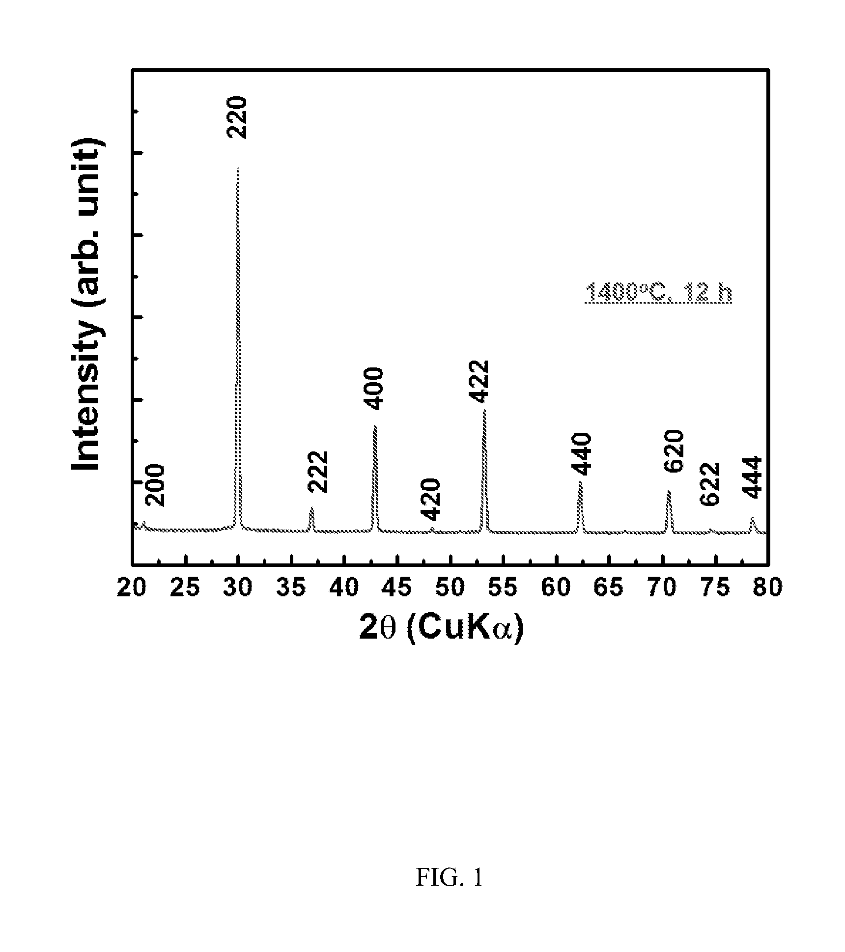
[0035]The invention incorporates a buffer layer of the double perovskite phase, such as Ba2(Y and / or RE)NbO6 or Ba2(Y and / or RE)TaO6, for growing the superconducting film. Since this phase has a large lattice mismatch with REBCO or YBC...


PUM


Abstract

A superconducting article includes a substrate having a biaxially textured surface. A biaxially textured buffer layer, which can be a cap layer, is supported by the substrate. The buffer layer includes a double perovskite of the formula A2B′B″O6, where A is rare earth or alkaline earth metal and B′ and B″ are different transition metal cations. A biaxially textured superconductor layer is deposited so as to be supported by the buffer layer. A method of making a superconducting article is also disclosed.

Description

STATEMENT REGARDING FEDERALLY SPONSORED RESEARCH OR DEVELOPMENT[0001]This invention was made with government support under DE-AC05-000822725 awarded by the United States Department of Energy. The Government has certain rights in the invention.FIELD OF THE INVENTION[0002]This invention relates to superconducting materials and more particularly to buffer layers for superconducting articles.BACKGROUND OF THE INVENTION[0003]Successful fabrication of biaxially textured superconducting wire based on the coated conductor technology requires optimization of the cost / performance of the HTS conductor. From a superconducting performance standpoint, a long, flexible, single crystal-like wire is required. From a cost and fabrication standpoint, an industrially scalable, low cost process is required. Both of these critical requirements are met by Rolling-assisted-biaxially-textured-substrates (RABiTS).[0004]In order for cost / performance for a conductor based on this technology to be optimized, fu...

Claims


Application Information

Patent Timeline
Patent Type & Authority Applications(United States)
IPC IPC(8): H01L39/12H01L39/24H01L39/02B05D5/12
CPCH01L39/126Y10T428/24355H01L39/24H01L39/2461H10N60/857H10N60/0632H01B12/00H10N60/01
Inventor GOYAL, AMITWEE, SUNG-HUN
Owner UNIV OF TENNESSEE RES FOUND
Why Eureka
Try Eureka