Compound semiconductor material and method for forming an active layer of a thin film transistor device

Inactive Publication Date: 2005-03-24
IND TECH RES INST
View PDF7 Cites 102 Cited by
  • Summary
  • Abstract
  • Description
  • Claims
  • Application Information

AI Technical Summary

Benefits of technology

[0007] The object of the present invention is to provide a compound semiconductor material for forming an active layer of a thin film transistor device so that the transistors of an active matrix flat panel display are high voltage-durable and have improv

Problems solved by technology

Currently, the thin film transistors (TFTs) are classified as the amorphous silicon TFTs and the low temperature polycrystalline silicon TFTs, both of which need to undergo the vacuum evaporation process and the photolithography process, and thus have a high manufacturing cost.
Although the Sol-gel process is simple and the materials used the

Method used


Image

  • Compound semiconductor material and method for forming an active layer of a thin film transistor device
  • Compound semiconductor material and method for forming an active layer of a thin film transistor device
  • Compound semiconductor material and method for forming an active layer of a thin film transistor device

Examples


embodiment 1

[0024] Embodiment 1

[0025] In the solution process, all of the oxides of group II-VI compounds can use 2-methoxy-ethanol or other alcohols as the solvent. When choosing the solvent, the factors concerned are the solubility of a solute, the ability for film formation of the solution, the removing of the solvent, and the growth of the grain.

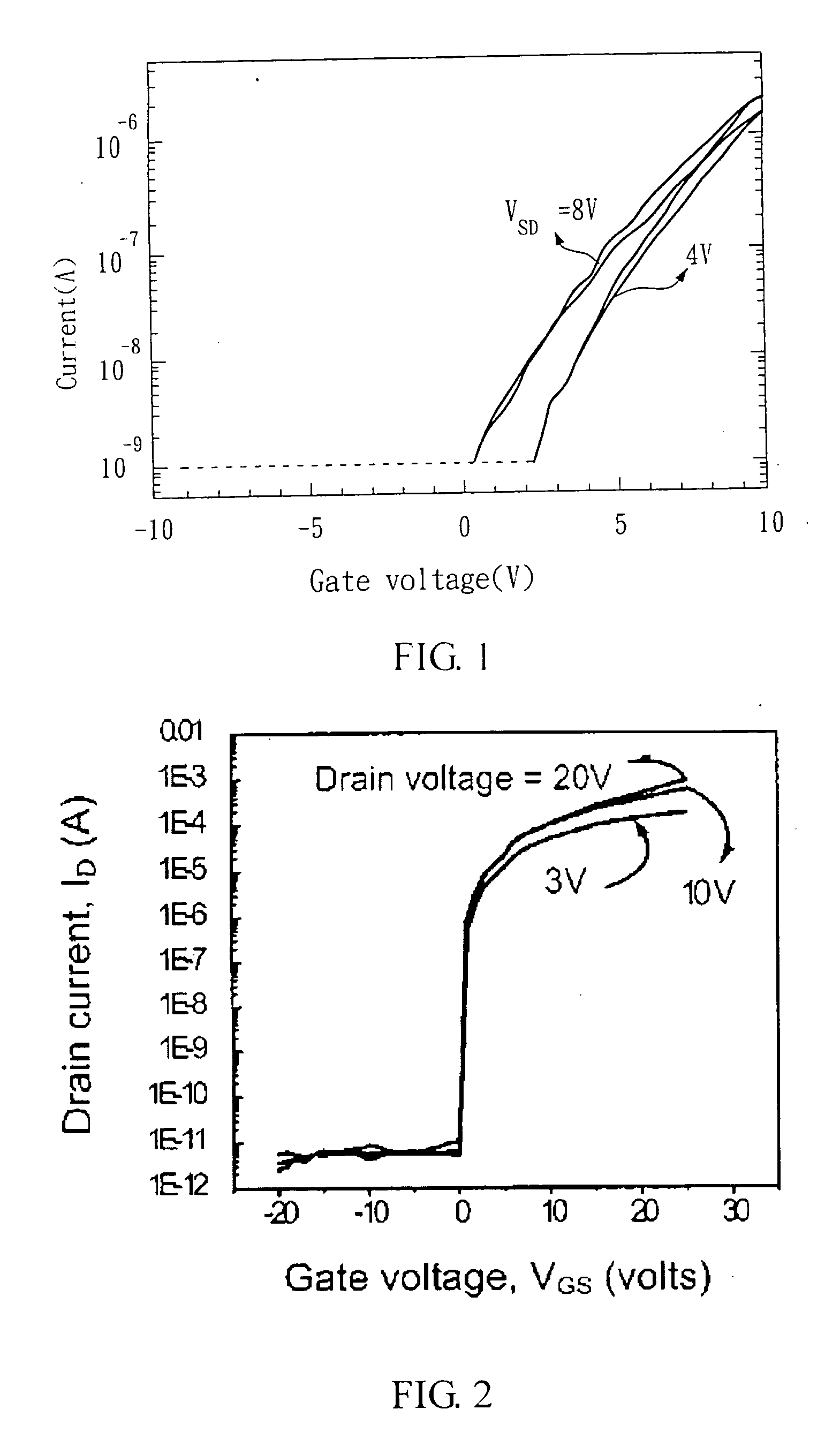
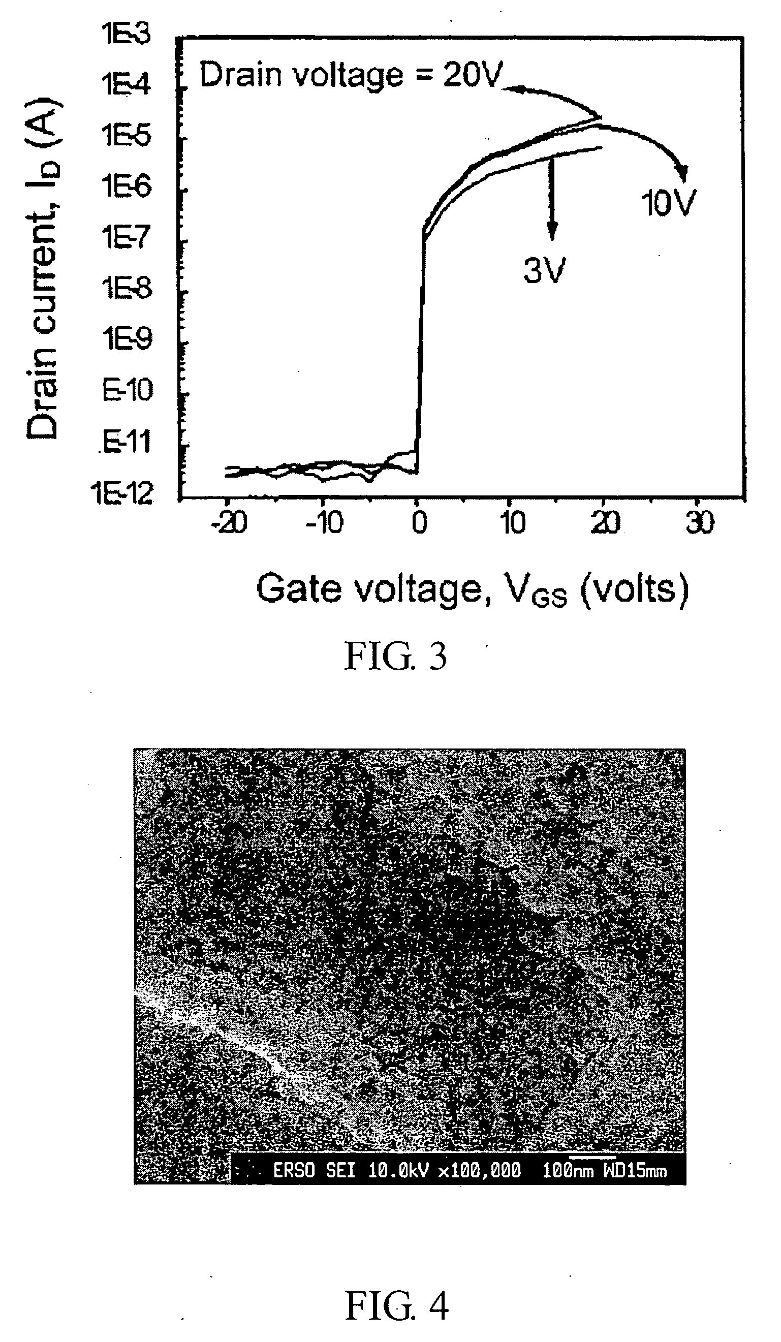
[0026] In the present embodiment, ZnO is doped with Mg to form a compound semiconductor material. First, 100 ml of solvent, i.e. 2-Methoxy-ethanol is mixed with 4.58 g of monoethanol amine. Then, 0.06 mole of zinc acetate and 0.015 mole of MgCl2 are further added into the solvent and stirred at 60 degrees C. for 30 minutes to prepare a precursor solution of Zn(0.8)Mg(0.2)O. Afterwards, the precursor solution is coated at the channels of the transistors by Inkjet Printing. Finally, the precursor solution coated at the channels of the transistors is annealed at 500 degrees C. for 2 hours in an oven. With reference to FIG. 4, the SEM picture shows tha...

embodiment 2

[0027] Embodiment 2

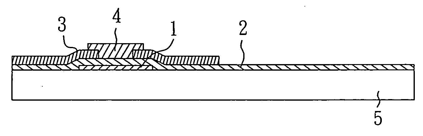
[0028] With reference to FIGS. 5A-5D, the process flow for manufacturing a thin film transistor is shown, wherein the bottom gate of the thin film transistor is formed with the compound semiconductor material of the present invention. As shown in FIG. 5A, a glass substrate 5 is provided, and then a first electrode layer is formed thereon. The first electrode layer is made of electrically conductive material, such as ITO, Cr, Al, Mo, Au, Pt, Ag, etc. Next, the first electrode layer is patterned by photolithography and etching processes and a gate electrode 1 is formed. As shown in FIG. 5B, an insulating layer 2 is subsequently deposited on the gate electrode 1. The insulating layer 2 can be made of silicon oxides, silicon nitrides, or PZT. The insulating layer 2 can be deposited by any conventional method. Preferably, the insulating layer 2 is deposited by physical vapor deposition or chemical vapor deposition. As shown in FIG. 5C, a second electrode layer 3 is for...


PUM


Abstract

A compound semiconductor material for forming an active layer of a thin film transistor device is disclosed, which has a group II-VI compound doped with a dopant ranging from 0.1 to 30 mol %, wherein the dopant is selected from a group consisting of alkaline-earth metals, group IIIA elements, group IVA elements, group VA elements, group VIA elements, and transitional metals. The method for forming an active layer of a thin film transistor device by using the compound semiconductor material of the present invention is disclosed therewith.

Description

BACKGROUND OF THE INVENTION [0001] 1. Field of the Invention [0002] The present invention relates to a compound semiconductor material and, more particularly, to a compound semiconductor material suitable for forming the active layer of a thin film transistor of an active matrix flat panel display. [0003] 2. Description of Related Art [0004] Recently, the active matrix flat panel display has become a popular focus for research and development. In particular, the emphasis of that research and development is directed to the thin film transistor. In addition to that, the flat panel display has been developed to have a large active area, a low price, and a high resolution. Currently, the thin film transistors (TFTs) are classified as the amorphous silicon TFTs and the low temperature polycrystalline silicon TFTs, both of which need to undergo the vacuum evaporation process and the photolithography process, and thus have a high manufacturing cost. Lately, a method for manufacturing a thi...

Claims


Application Information

Patent Timeline
IPC IPC(8): H01L21/336H01L29/786
CPCH01L29/66969H01L29/7869
Inventor HO, JIA-CHONGLEE, JEN-HAOLEE, CHENG-CHUNGWANG, YU-WULEE, CHUN-TAOLIN, PANG
Owner IND TECH RES INST
Why Eureka
Try Eureka