

UV assisted silylation for recovery and pore sealing of damaged low k films
a low k film, pore sealing technology, applied in the direction of basic electric elements, semiconductor/solid-state device manufacturing, electric apparatus, etc., can solve the problems of increasing the k value, affecting the resistive capacitance and reliability of the dielectric film, and modifying the film structur
- Summary
- Abstract
- Description
- Claims
- Application Information
AI Technical Summary
Benefits of technology
Problems solved by technology
Method used
Image

Examples
Embodiment Construction
[0012]Embodiments of the present invention generally relate to methods for repairing and lowering the dielectric constant (k-value) of low k films for semiconductor fabrication.
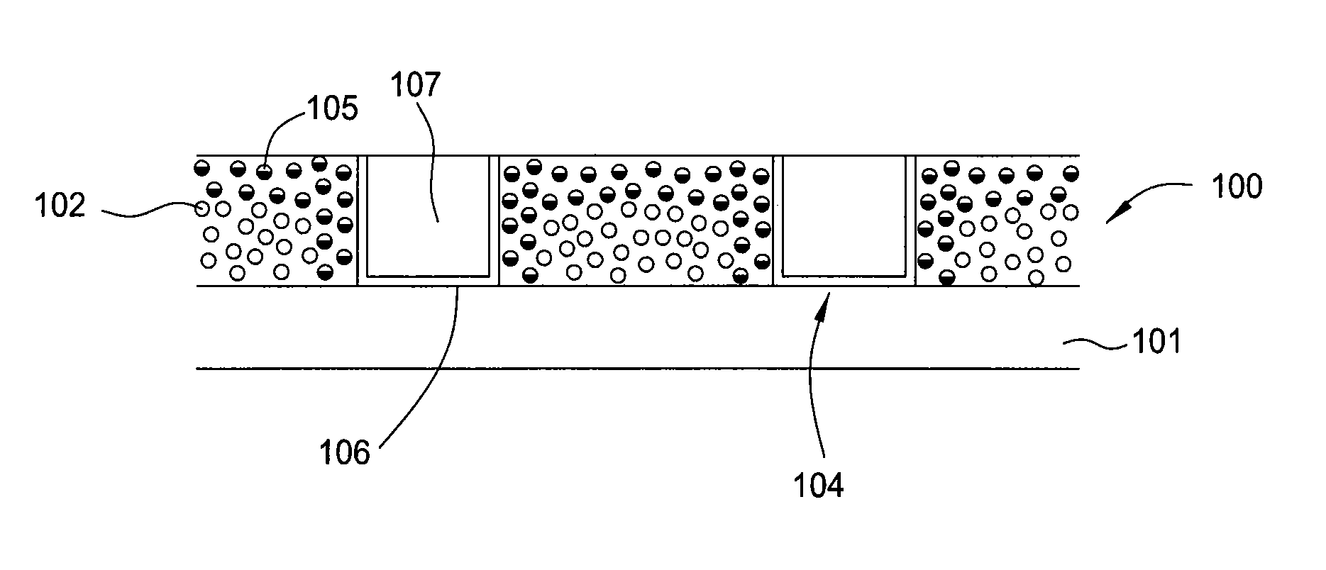
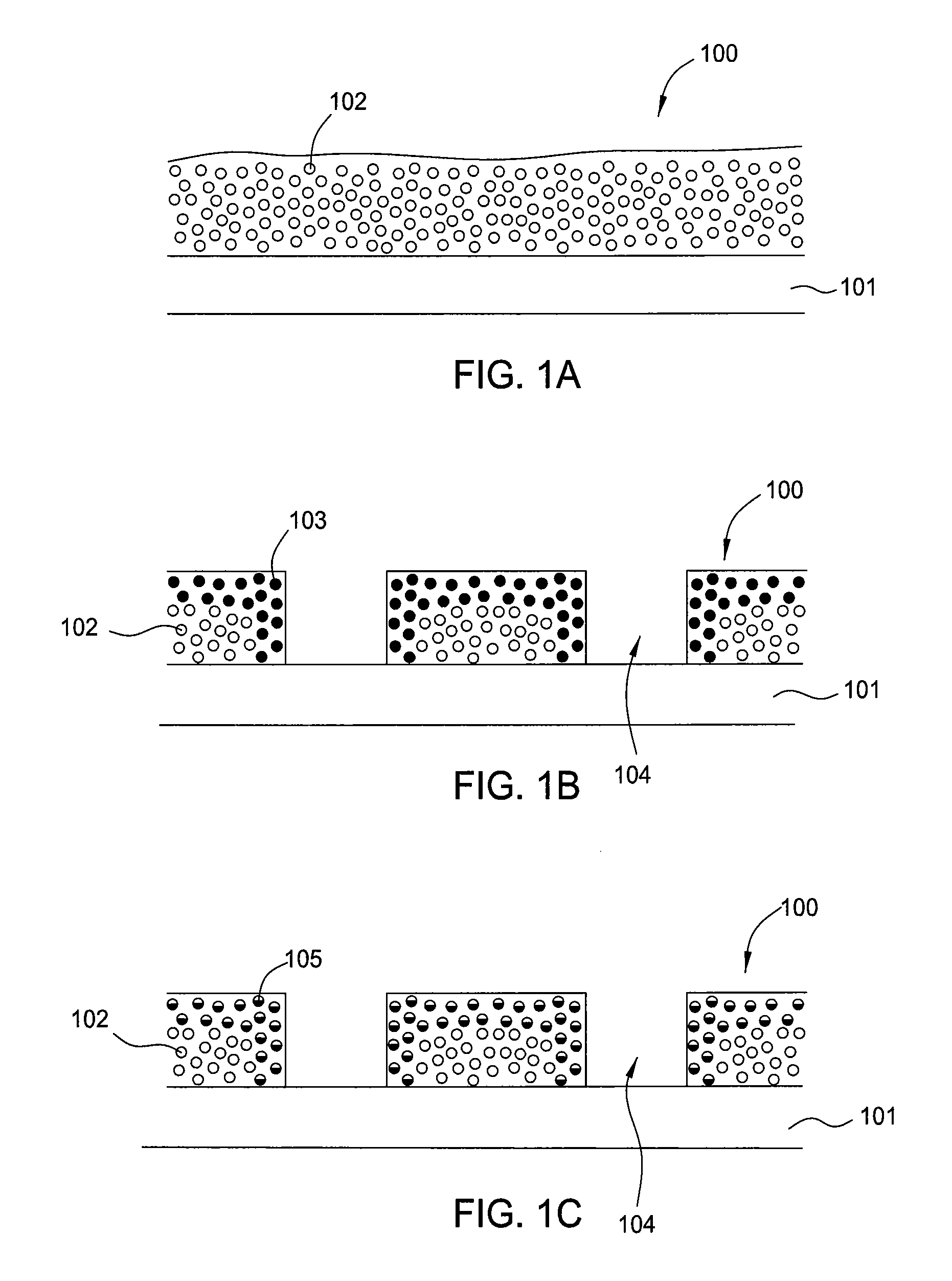
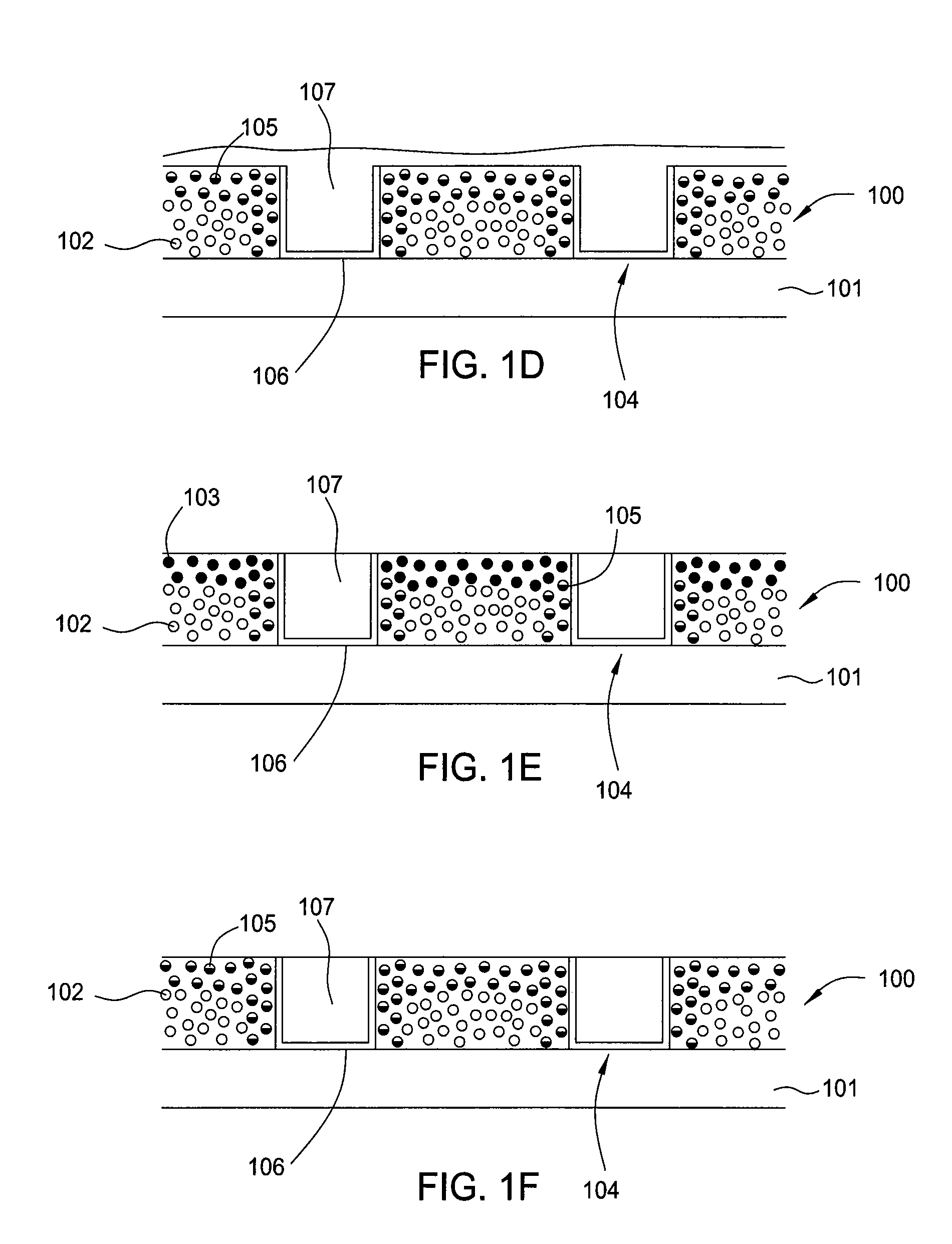
[0013]FIG. 1A illustrates a dielectric film 100 deposited onto a structure 101. The structure 101 may be a substrate, such as, for example, a silicon wafer, or a previously formed layer, such as, for example, a metallization or interconnect layer. The dielectric film 100 may be a porous silicon containing low k film, such as, for example, SiO2, SiOC, SiON, SiCOH, SiOCN, or other related films. The dielectric film 100 may have pores 102 formed therein.
[0014]FIG. 1B illustrates the dielectric film 100 after being planarized and etched to form features 104 into the dielectric film 100. The dielectric film 100 may be planarized by a chemical mechanical planarization (CMP) process, for example. The dielectric film 100 may be etched by masking a portion of the dielectric film 100, contacting the unmasked portion of...
PUM
 Abstract
Description
Claims
Application Information