Display device

a display module and liquid crystal technology, applied in static indicating devices, instruments, optical elements, etc., can solve the problems of unfavorable excess power consumption, low transmittance of display modules, and inability to properly drive liquid crystal molecules in the blue phase lcd, etc., to achieve low transmittance and high driving voltage

Inactive Publication Date: 2012-11-08
AU OPTRONICS CORP +1
View PDF13 Cites 9 Cited by
  • Summary
  • Abstract
  • Description
  • Claims
  • Application Information

AI Technical Summary

Benefits of technology

[0010]In the display device according to an exemplary embodiment of the invention, the compensation films are disposed between the top polarizer and bottom polarizer. The configuration of the compensation films can adjust the polarization state of the directional light entering the display module, such that the polarization state of the directional light matches the absorption axis direction of the top polarizer. Accordingly, light leakage can be minimized and the contrast ratio and viewing angle of the display device can be enhanced.

Problems solved by technology

However, in the electrode design of a typical IPS display module, many regions above the electrodes do not have transverse electric fields.
Consequently, a plurality of liquid crystal molecules in the blue phase LCD cannot be properly driven, such that the transmittance of the display module is low.
Although the transmittance of the IPS display module can be enhanced by increasing the driving voltage, the resulting excess power consumption is unfavorable.

Method used


Image

  • Display device
  • Display device
  • Display device

Examples


first embodiment

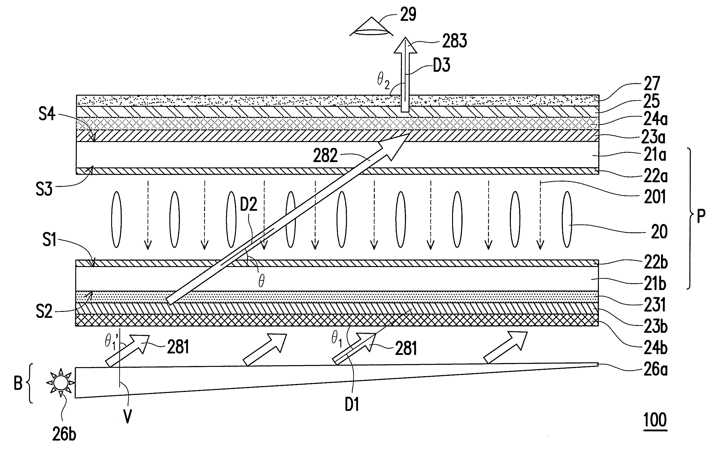
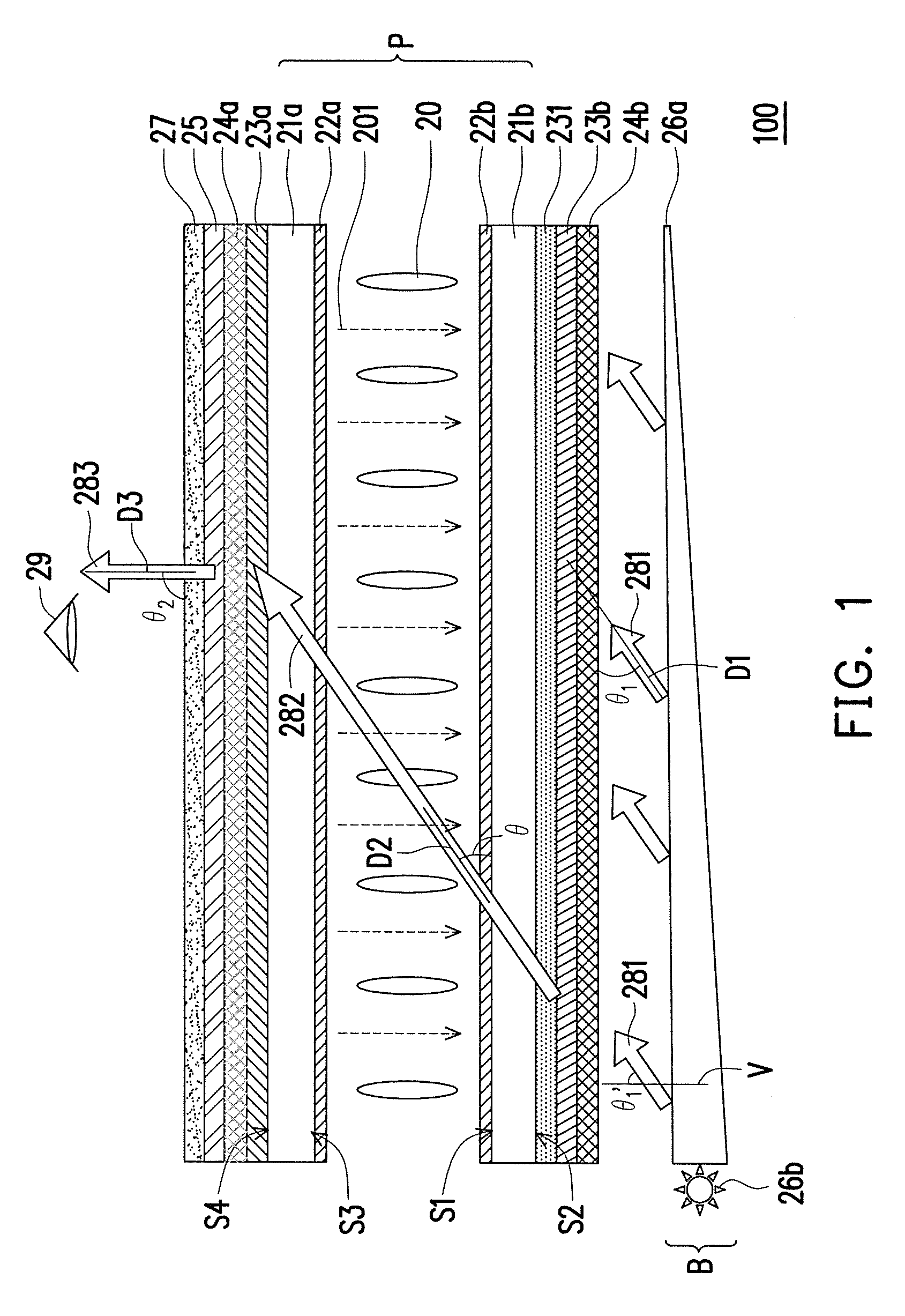
[0123]FIG. 21 is a schematic cross-sectional view of a display device according to a first embodiment of the invention. With reference to FIG. 21, a difference between a display device 100a and the embodiment of FIG. 1 lies in that, the display device 100a includes a first compensation film 28b and a second compensation film 28a, and does not include the compensation film 231. To be specific, the first compensation film 28b is disposed on the outer surface S2 of the first substrate 21b, and the second compensation film 28a is disposed between the second substrate 21a and the turning optical film 25.

[0124]In the present embodiment, the bottom polarizer 23b is disposed on the outer surface S2 of the first substrate 21b, and the top polarizer 23a is disposed on the outer surface S4 of the second substrate 21a. According to the present embodiment, the bottom polarizer 23b is disposed between the first compensation film 28b and the first optical film 24b. The top polarizer 23a is dispose...

second embodiment

[0138]FIG. 30 is a schematic cross-sectional view of a display device according to a second embodiment of the invention. With reference to FIG. 30, a display device 100b of the present embodiment is similar to the display device 100a of the first embodiment. A difference therebetween lies in that, the display device 100b further includes a third compensation film 31b and a fourth compensation film 31a. The third compensation film 31b is disposed between the first compensation film 28b and the bottom polarizer 23b, and the fourth compensation film 31a is disposed between the second compensation film 28a and the top polarizer 23a.

[0139]According to the present embodiment, the third compensation film 31b and the fourth compensation film 31a are respectively a biaxial compensation film, for example. The third compensation film 31b and the fourth compensation film 31a may be designed in accordance with different orientation angle Φ, so as to compensate for an angular difference between ...

third embodiment

[0142]FIG. 33 is a schematic cross-sectional view of a display device according to a third embodiment of the invention. With reference to FIG. 33, a display device 100c of the present embodiment is similar to the display device 100b of the second embodiment. A difference therebetween lies in that, in the display device 100c, the third compensation film 31b is disposed between the first compensation film 28b and the first substrate 21b, and the fourth compensation film 31a is disposed between and the second compensation film 28a and the second substrate 21a.

[0143]According to the present embodiment, the third compensation film 31b and the fourth compensation film 31a are respectively a biaxial compensation film, for example. The third compensation film 31b and the fourth compensation film 31a may be designed in accordance with different orientation angles Φ, so as to compensate for an angular difference between the top polarizer 23a and the bottom polarizer 23b. According to the pre...


PUM

PropertyMeasurementUnit
orientation angleaaaaaaaaaa

Abstract

A display device including a display module, a light source module, a turning optical film, a first compensation film and a second compensation film is provided. The display module includes a first substrate, a second substrate and a display medium. The light source module generates directional light. The display module is disposed above the light source module. The second substrate is disposed opposite to the first substrate. The display medium is disposed between the first substrate and the second substrate and is optically isotropic. The turning optical film is disposed on the second substrate of the display module. The directional light enters the turning optical film and then exits the turning optical film to form an output light. The first compensation film is disposed on the first outer surface of the first substrate. The second compensation film is disposed between the second substrate and the turning optical film.

Description

CROSS-REFERENCE TO RELATED APPLICATION[0001]This application claims the priority benefits of U.S. provisional application Ser. No. 61 / 481,295, filed on May 2, 2011 and Taiwan application serial no. 101114566, filed on Apr. 24, 2012. The entirety of each of the above-mentioned patent applications is hereby incorporated by reference herein and made a part of this specification.BACKGROUND OF THE INVENTION[0002]1. Field of the Invention[0003]The invention relates to a display device, and more particularly to a liquid crystal display device.[0004]2. Description of Related Art[0005]With vigorous development of display technologies, consumers' requirements for favorable performance of displays have been increasing. Specifically, consumers have high demands for the response time of the displays in addition to the requirements for resolution, contrast ratio, viewing angle, grey level inversion, and color saturation.[0006]To satisfy said requirements, blue phase liquid crystal displays (LCDs)...

Claims


Application Information

Patent Timeline
Patent Type & Authority Applications(United States)
IPC IPC(8): G09G3/36G06F3/038
CPCG02F1/1334G02F1/133524G02F1/1336G02B6/0053G02F2001/133562G02F2001/13793G02F1/1393
Inventor CHENG, HUI-CHUANYAN, JINISHINABE, TAKAHIROWU, SHIN-TSONLIN, CHING-HUANLIU, KANG-HUNG
Owner AU OPTRONICS CORP
Why Eureka
Try Eureka