Semiconductor chip module and planar stack package having the same

a semiconductor chip and chip module technology, applied in the field of semiconductor packages, can solve the problems of difficult to reduce the size of the memory chip mounted package, difficult to achieve target processability and reliability, etc., to achieve the effect of ensuring the processability of the package manufacturing process and the reliability of the packag

Inactive Publication Date: 2012-11-15
SK HYNIX INC
View PDF4 Cites 5 Cited by
  • Summary
  • Abstract
  • Description
  • Claims
  • Application Information

AI Technical Summary

Benefits of technology

[0007]An embodiment of the present invention is directed to a semiconductor chip module that ca

Problems solved by technology

In this regard, since limitations exist in increasing the capacity of a semiconductor chip itself, a stack package has been developed such that a required capacity can be achieved by vertically stacking at least two semiconductor chips in one package.
However, although the size of a memo

Method used


Image

  • Semiconductor chip module and planar stack package having the same
  • Semiconductor chip module and planar stack package having the same
  • Semiconductor chip module and planar stack package having the same

Examples


Embodiment Construction

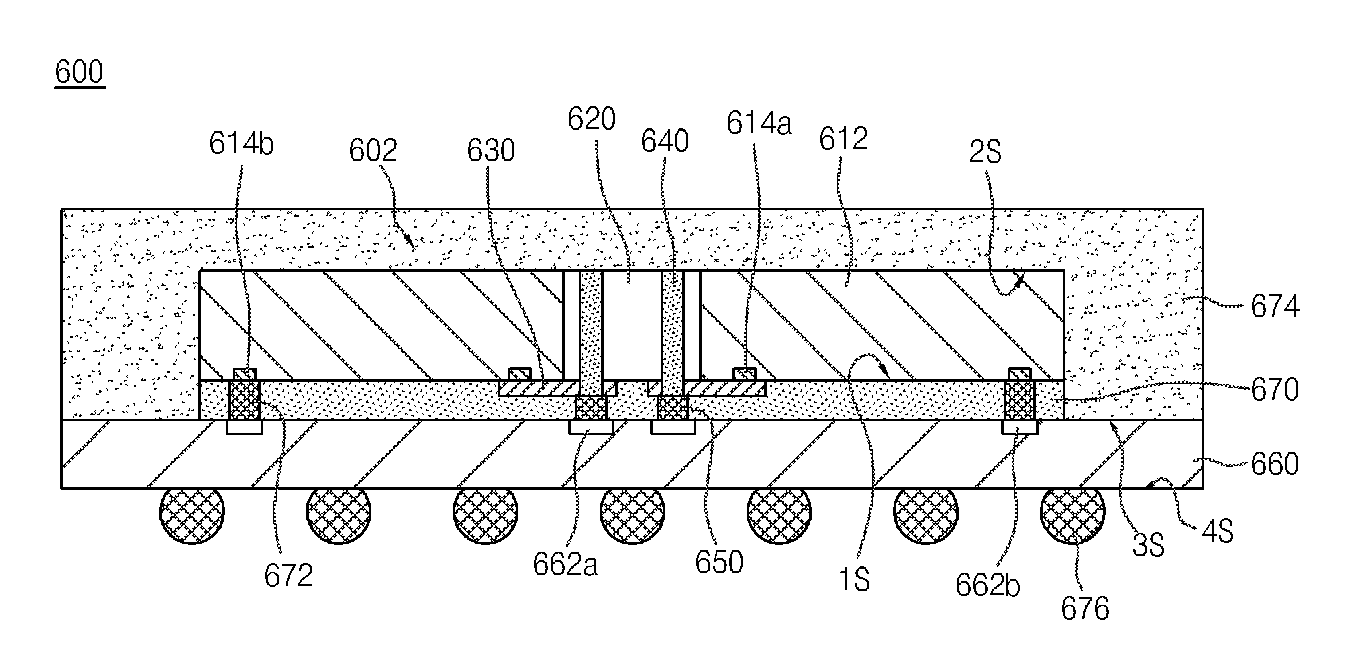
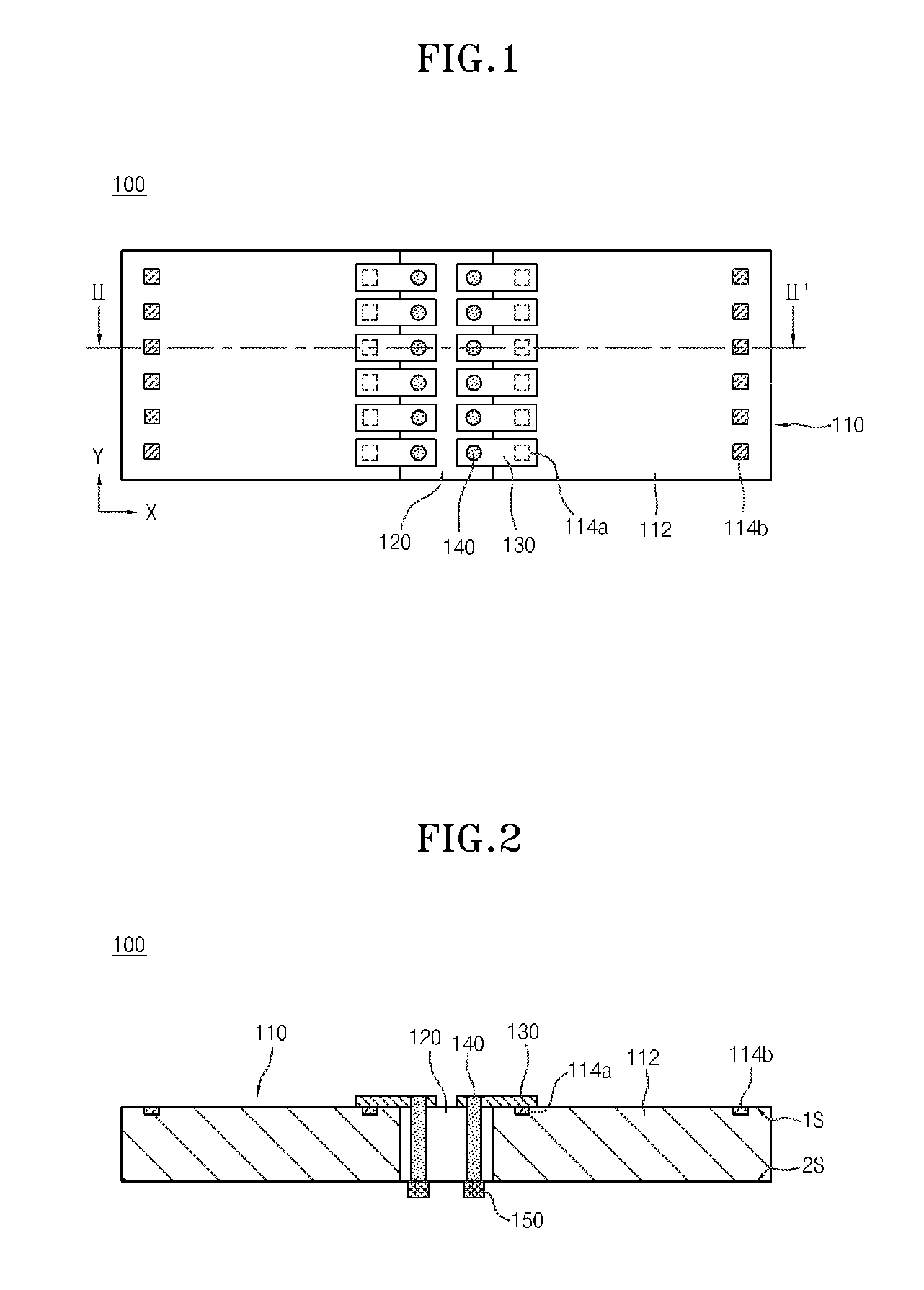
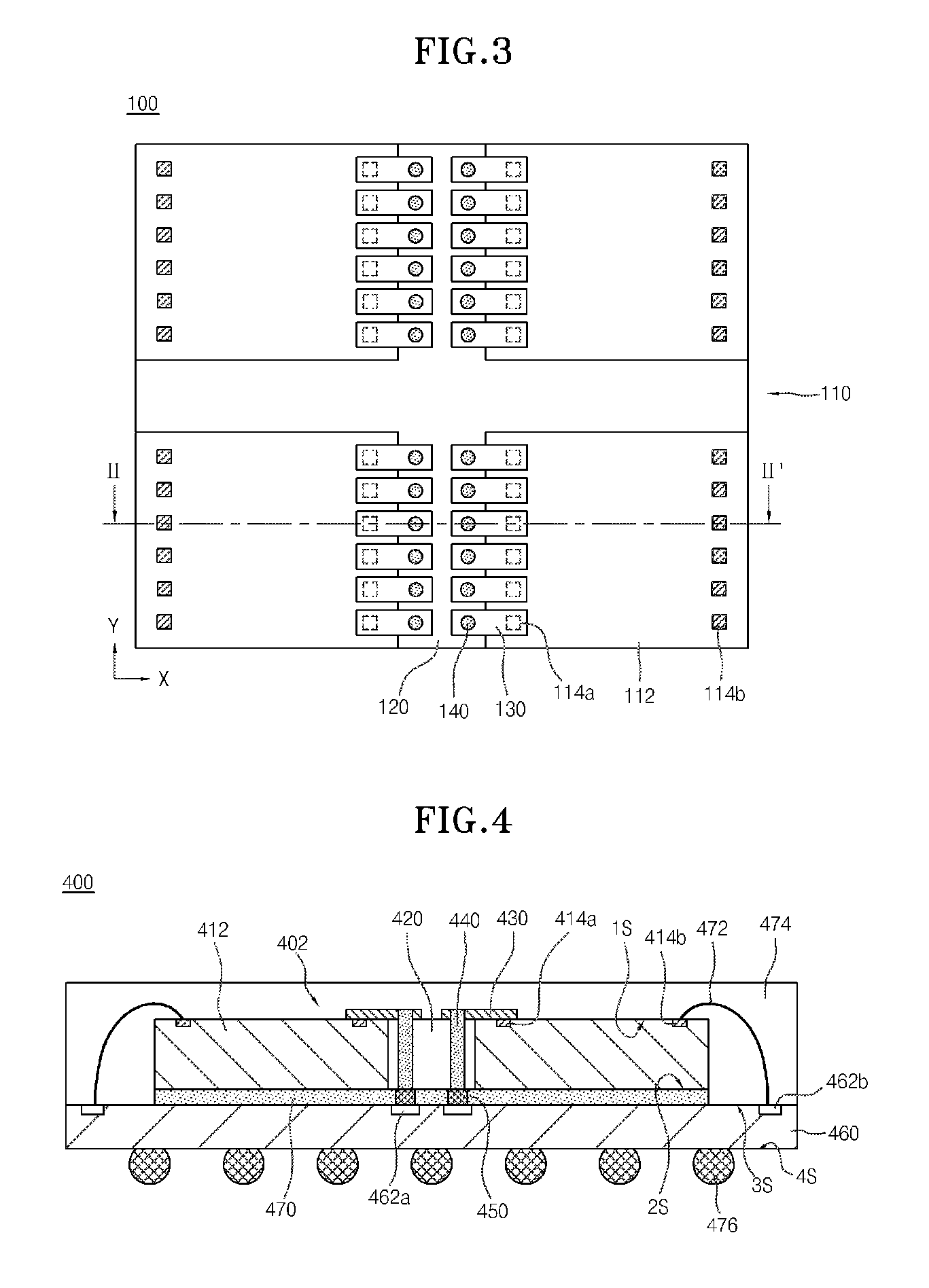
[0035]In various embodiments of the present invention, a semiconductor chip module is constructed by sawing at least two semiconductor chips completely manufactured at a wafer level, and a planar stack package is realized by applying the semiconductor chip module constructed in this way.

[0036]Accordingly, various embodiments of the present invention can increase capacity even with the same chip size. In particular, it is possible to overcome a limitation in ball pitch, and since semiconductor chips and a substrate are electrically connected using the space of a scribe lane, processability and reliability can be secured.

[0037]Hereafter, specific embodiments of the present invention will be described in detail with reference to the accompanying drawings.

[0038]It is to be understood herein that the drawings are not necessarily to scale and in some instances proportions may have been exaggerated in order to more clearly depict certain features of the invention.

[0039]FIG. 1 is a plan vie...


PUM


Abstract

A semiconductor chip module includes a chip unit including at least two semiconductor chips disposed with a scribe lane interposed therebetween and each of which has a first surface on which bonding pads are disposed and a second surface that faces away from the first surface. Redistribution lines formed on the first surface of each semiconductor chip have first ends, which are connected with the bonding pads of each semiconductor chip, and second ends that extend to and are disposed on the scribe lane. Through electrodes formed to pass through the scribe lane are electrically connected with the second ends of the redistribution lines.

Description

CROSS-REFERENCE TO RELATED APPLICATIONS[0001]The present application claims priority to Korean patent application number 10-2011-0044097 filed on May 11, 2011, which is incorporated herein by reference in its entirety.BACKGROUND OF THE INVENTION[0002]The present invention relates to a semiconductor package, and more particularly, to a semiconductor chip module and a planar stack package having the same, while securing the processability of a package manufacturing process and the reliability of a package.[0003]A semiconductor package has been developed to decrease its size and to improve its electrical characteristics. A typical example of such a semiconductor package includes a ball grid array (BGA) package. The BGA package has a structure in which a semiconductor chip is disposed on the upper surface of a substrate, the upper surface of the substrate including the semiconductor chip is then sealed, and a plurality of solder balls are attached as external connection terminals to the...

Claims


Application Information

Patent Timeline
IPC IPC(8): H01L23/544
CPCH01L23/481H01L2924/01029H01L24/73H01L2224/16225H01L2224/32225H01L2224/48227H01L2224/73204H01L2224/73265H01L23/49816H01L2924/15311H01L2924/00013H01L2224/73257H01L2224/131H01L2224/13025H01L2224/06182H01L2224/04042H01L2224/0401H01L2224/02371H01L24/06H01L2224/02372H01L2224/02377H01L2924/00H01L2224/13099H01L2224/13599H01L2224/05599H01L2224/05099H01L2224/29099H01L2224/29599H01L2924/014H01L2924/00012H01L2924/181H01L2224/96H01L23/48H01L23/12H01L21/78
Inventor LEE, SEUNG YEOP
Owner SK HYNIX INC
Why Eureka
Try Eureka