Laser Array Light Source Unit

a technology of laser array light source unit and light source unit, which is applied in the direction of lasers, semiconductor laser structural details, semiconductor lasers, etc., can solve the problems of difficult application to image display systems, and achieve the effect of efficiently releasing heat generated, reducing the size of cooling devices, and reducing the size of laser array light source units

Active Publication Date: 2012-11-15
PANASONIC CORP
View PDF3 Cites 26 Cited by
  • Summary
  • Abstract
  • Description
  • Claims
  • Application Information

AI Technical Summary

Benefits of technology

[0027]With this structure of the present invention, the size of the cooling device can be reduced, and as a result, the size of the laser array light source unit itself can also be reduced.
[0028]The present invention can provide a laser array light source unit having a structure that can efficiently release heat generated from semiconductor la...

Problems solved by technology

In the past, solid light sources such as LEDs and semiconductor lasers have been considered, due ...

Method used


Image

  • Laser Array Light Source Unit
  • Laser Array Light Source Unit
  • Laser Array Light Source Unit

Examples


first embodiment

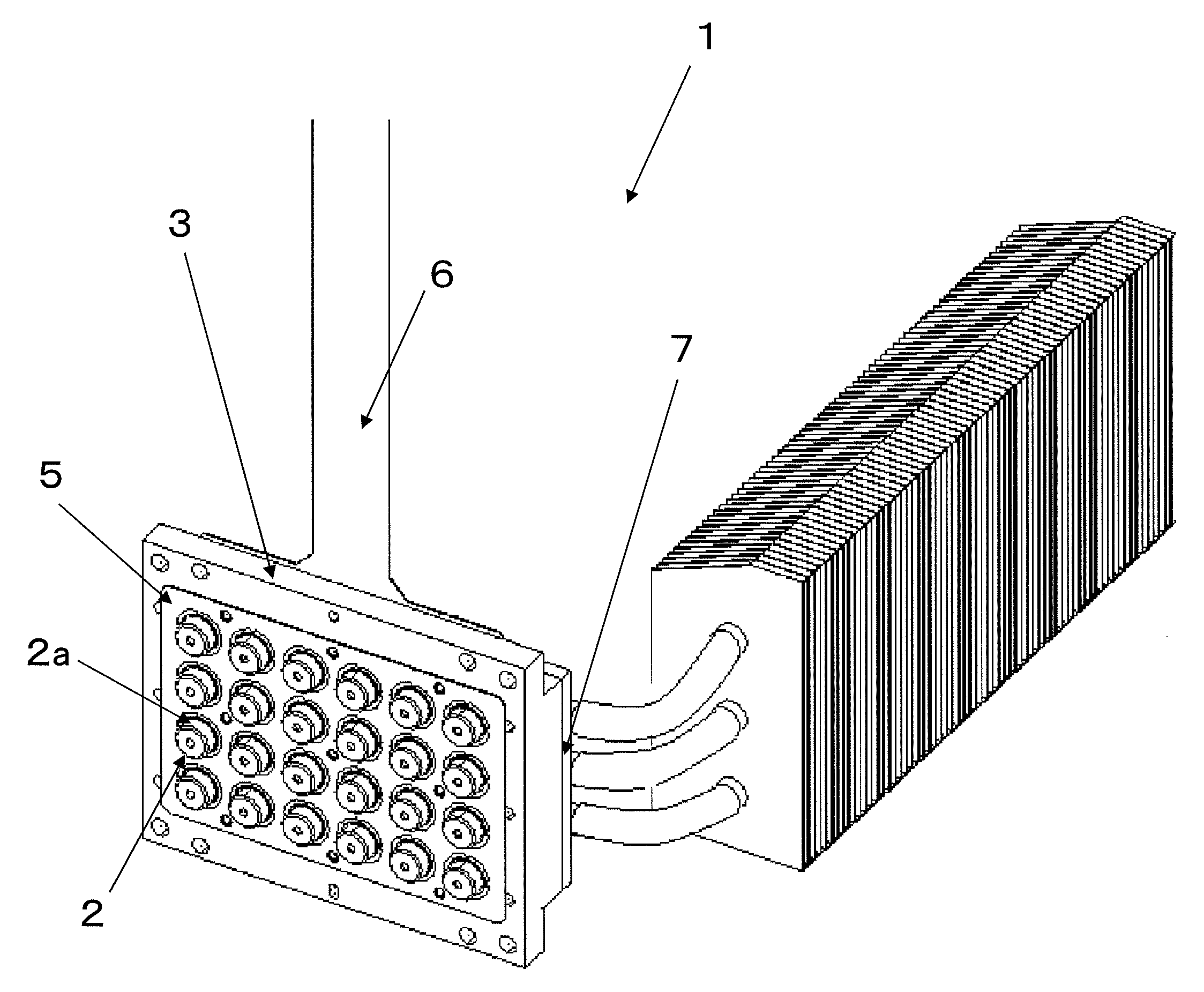
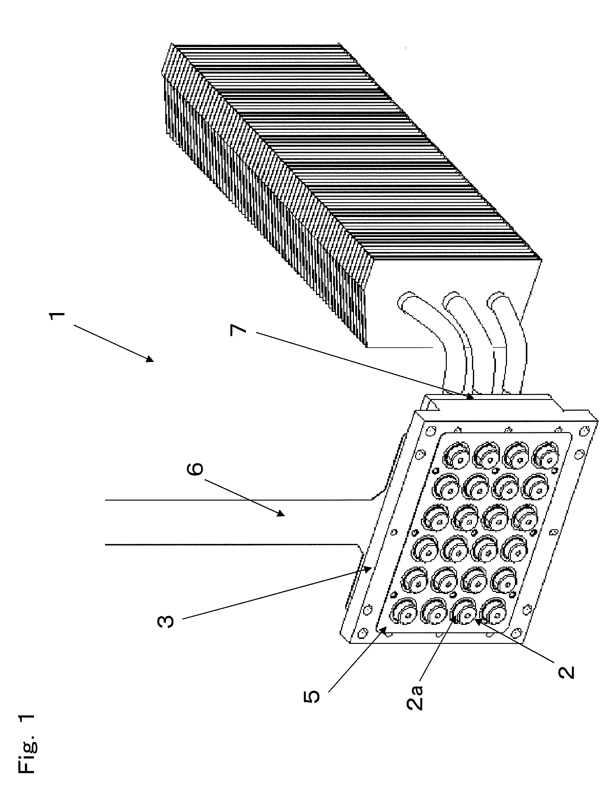
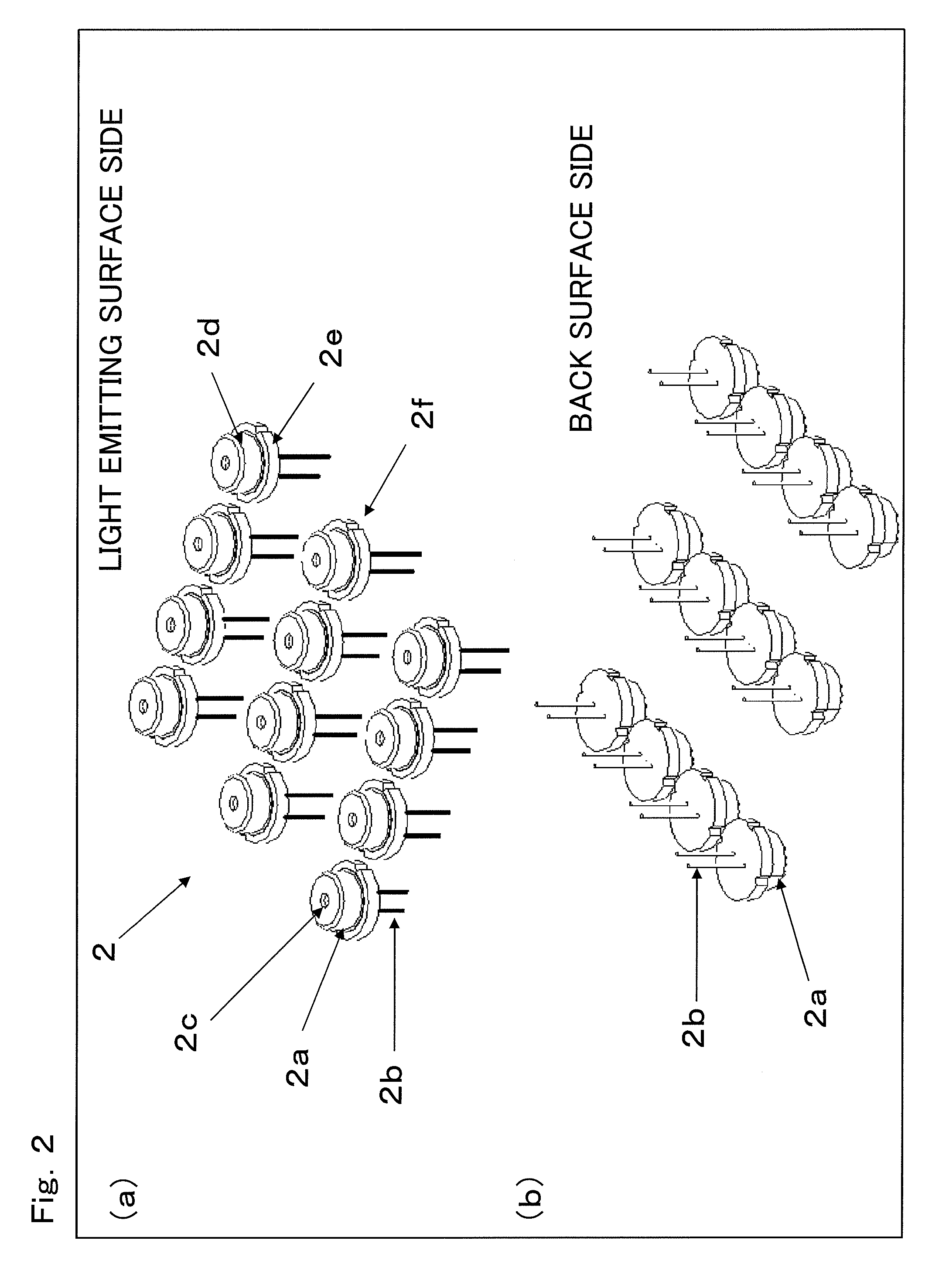
[0045]Hereinafter, a laser array light source unit 1 according to the present embodiment will be described with reference to the drawings. FIG. 1 illustrates the laser array light source unit 1 according to the present embodiment. FIG. 2 illustrates semiconductor lasers 2 according to the present embodiment. FIG. 2(a) is a perspective view of the semiconductor lasers 2 according to the present embodiment, as viewed from their light-emitting surface side, and FIG. 2(b) is a perspective view of the semiconductor lasers 2 according to the present embodiment, as viewed from their back surface side. FIG. 3 illustrates a laser holder 3 according to the present embodiment. FIG. 4 illustrates an insulator 4 according to the present embodiment. FIG. 4(a) is a perspective view of the insulator 4 according to the present embodiment, and FIG. 4(b) is a view of the insulator 4 cut along a A-A line shown in FIG. 4(a). FIG. 4(c) is an enlarged cross-sectional view of the through-hole 4a of the ins...

second embodiment

[0075]A structure of a laser array light source unit according to the present embodiment will be described with reference to FIG. 8. FIG. 8 illustrates positions of a wiring base 6 and a laser holder 3 according to the present embodiment. As shown in FIG. 8, the wiring base 6 has second through-holes 6d different from first through-holes 6c into which leading electrodes are inserted. Reference pins 3e provided in the laser holder 3 pass through the second through-holes 6d. The first through-holes 6c of the wiring base 6 are located so as to correspond to through-holes 4a of the insulator 4 in a state where the reference pins 3e have passed through the second through-holes 6d. Components other than these can be the same as described in the first embodiment, and thus are denoted by the same reference characters, and the description thereof is omitted.

[0076]By passing the reference pins 3e of the laser holder 3 through the second through-holes 6d provided in the wiring base 6 as descri...

third embodiment

[0077]A structure of a laser array light source unit according to the present embodiment will be described with reference to FIG. 9A and FIG. 9B. FIG. 9A illustrates positions of a wiring base 6, a laser holder 3, and a jig 8, and FIG. 9B illustrates the positions of the wiring base 6 and the laser holder 3. FIG. 9B is for illustrating the positional relationship between the wiring base 6 and the laser holder 3 in a state where the jig 8 is removed. The jig 8 described herein is a component used when the laser array light source unit is to be built in an actual production process.

[0078]In this case, as shown in FIG. 9A, the wiring base 6 has second through-holes 6d different from first through-holes 6c into which leading electrodes are inserted. Reference pins 8a provided in the jig 8 pass through reference holes 3d provided in the laser holder 3 and further pass through the second through-holes 6d. The first through-holes 6c of the wiring base 6 are located so as to correspond to t...


PUM


Abstract

A laser array light source unit 1 includes: a plurality of semiconductor lasers 2 each including a main body portion 2a and a leg portion 2b with two leading electrodes; a laser holder 3 holding the main body portions 2a, and having through-holes for the leg portions 2b; a pressing member 5 for fixing the semiconductor lasers 2 to the laser holder 3; an insulator 4 including a plurality of electrode insertion portions 4f having through-holes for the leading electrodes; and a wiring base 6 for electrically connecting at least two of the semiconductor lasers 2 in series. The insulator 4 includes a connecting portion 4b for connecting the plurality of electrode insertion portions 4f in the same direction in which the plurality of semiconductor lasers 2 are arranged. The wiring base 6 includes first through-holes into which the leading electrodes of the semiconductor lasers 2 are inserted.

Description

BACKGROUND OF THE INVENTION[0001]1. Field of the Invention[0002]The present invention relates to laser array light source units, and more particularly relates to a laser array light source unit configured to efficiently release heat generated from a plurality of semiconductor lasers.[0003]2. Description of the Background Art[0004]As means for efficiently obtaining large images, projection-type image display devices such as projectors are conventionally used that irradiate a spatial light modulation element, such as a small DMD (Digital Micromirror Device) for forming images based on video signals, with light from a light source such as a mercury lamp, and magnifies and projects an optical image on a screen by use of a projection lens.[0005]In the past, solid light sources such as LEDs and semiconductor lasers have been considered, due to their insufficient brightness, to be difficult to apply to image display systems such as projectors. Nowadays, however, the use of these solid ligh...

Claims


Application Information

Patent Timeline
IPC IPC(8): H01S5/024
CPCH01S5/02H01S5/02212H01S5/02469H04N9/3164H04N9/3111H04N9/3161H01S5/4025
Inventor SARUWATARI, NAOTOYAMAGISHI, SHIGEKAZUNANBA, SHUSAKATANI, SHIGEAKIYUKIMOTO, FUMIO
Owner PANASONIC CORP
Why Eureka
Try Eureka